

Surface Chemistry and Composition Analysis Services (XPS/EDS)
The surface of a nanomaterial represents its primary interface with the surrounding world. Whether the goal is drug delivery, catalysis, sensing, or composite reinforcement, surface chemistry dictates how nanoparticles interact with biological systems, chemical reagents, and matrix materials. Understanding this chemistry at the atomic level is not merely informative, it is transformative.
At Eata Nanomaterials, we offer a comprehensive suite of surface analysis services centered on two complementary techniques: X-ray photoelectron spectroscopy (XPS) for quantitative surface chemistry and chemical state analysis, and energy-dispersive X-ray spectroscopy (EDS) for rapid elemental identification and spatial mapping. Together, these techniques provide a complete picture of what elements reside on a nanomaterial surface, how they are chemically bonded, and where they are distributed.
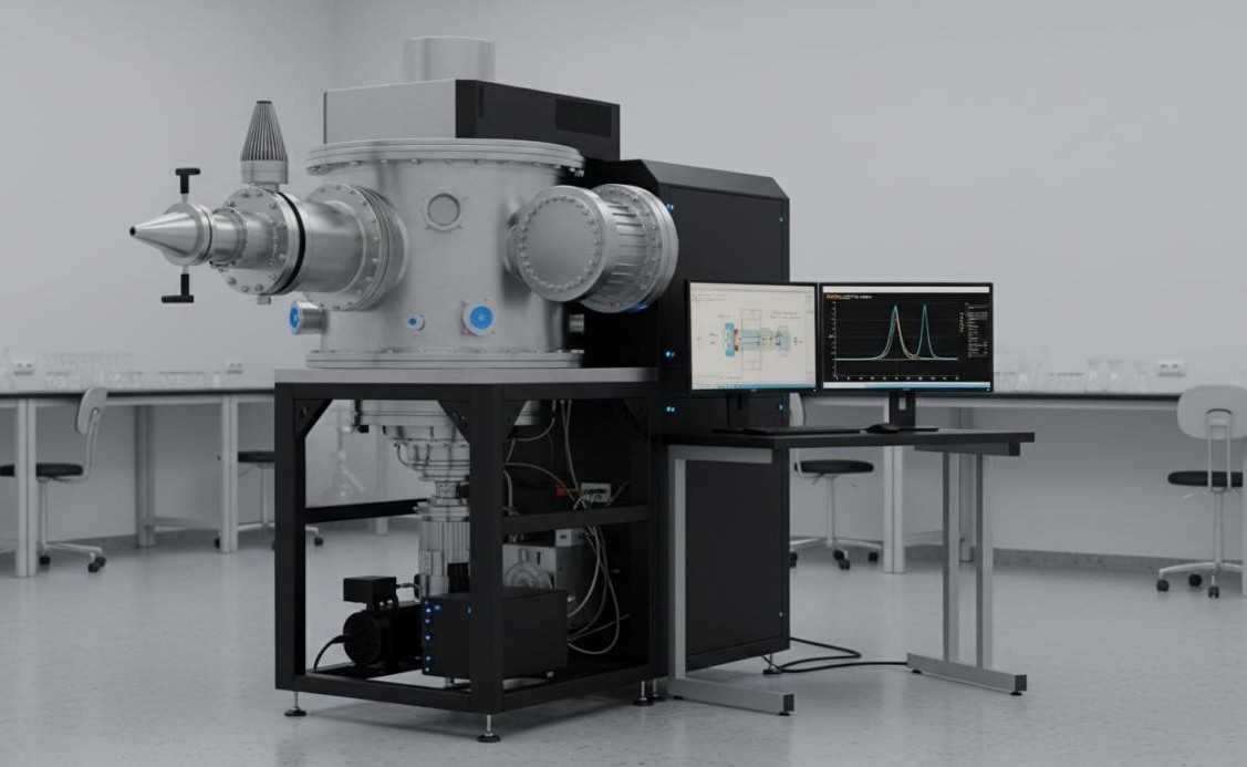 Figure 1: An X-ray photoelectron spectroscopy system with analytical chamber, X-ray source, and electron energy analyzer.
X-Ray Photoelectron Spectroscopy for Quantitative Surface Chemistry
XPS operates on Einstein's photoelectric principle. Monochromatic X-rays, typically Al K-alpha at 1486.6 eV, irradiate the sample surface, exciting and ejecting electrons from inner atomic orbitals. The kinetic energy of these emitted photoelectrons is measured by an electrostatic analyzer, and their binding energy is calculated. Because binding energies are characteristic of both element and chemical environment, XPS simultaneously identifies which elements are present and how they are chemically bonded.
The extreme surface sensitivity of XPS, probing only the top 1 to 10 nanometers, makes it uniquely suited for nanomaterial characterization where surface properties dominate behavior. The technique is quantitative, non-destructive, and capable of detecting all elements except hydrogen and helium.
Our XPS analysis services encompass:
- Elemental composition analysis quantifying the atomic percentage of each element present on the surface with detection limits typically around 0.1 atomic percent
- Chemical state determination resolving different oxidation states and bonding environments of the same element through binding energy shifts, such as distinguishing Fe2+ from Fe3+ in iron oxide nanoparticles
- Functional group identification confirming the presence of specific surface chemistries including carboxyl, hydroxyl, amine, thiol, and carbonyl groups on functionalized nanomaterials
- Angle-resolved XPS (ARXPS) providing non-destructive depth profiling of ultrathin films by varying the photoelectron collection angle to probe different sampling depths
- Sputter depth profiling using monatomic argon or gas cluster ion beams to remove material layer by layer, generating compositional profiles through multilayer coatings and core-shell architectures
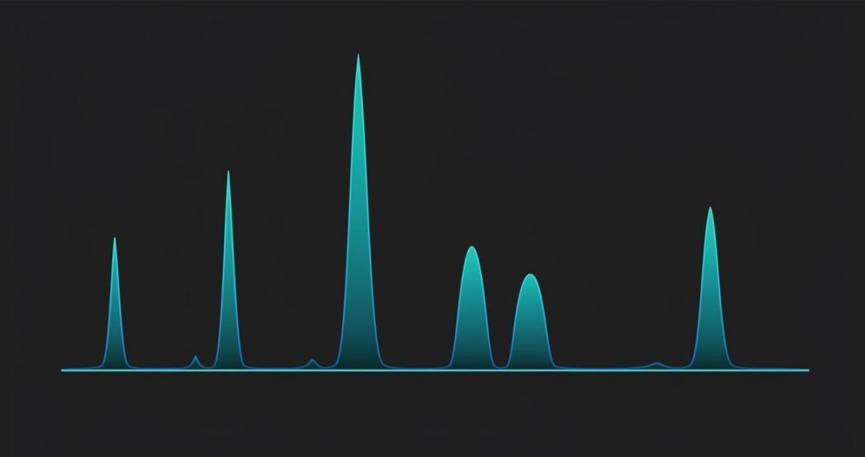 Figure 2: A representative XPS spectrum showing multiple characteristic peaks corresponding to different elements and chemical states on a nanomaterial surface.
Energy-Dispersive X-Ray Spectroscopy for Elemental Identification and Mapping
EDS detects characteristic X-rays emitted when a sample is bombarded with a high-energy electron beam in a scanning or transmission electron microscope. Each element in the periodic table produces X-rays at unique energy levels corresponding to electronic transitions between atomic shells. A silicon drift detector captures these X-rays and constructs an energy spectrum revealing the elemental composition of the analyzed region.
When coupled with electron microscopy, EDS achieves spatial resolutions extending to the nanometer scale, enabling elemental analysis of individual nanoparticles, interfaces, and nanoscale features that bulk techniques cannot resolve.
Our EDS capabilities include:
- Point analysis determining the elemental composition of a specific location as small as a few nanometers when operated in scanning transmission electron microscopy mode
- Line scanning tracking elemental concentration variations along a defined path across a sample, ideal for profiling compositional gradients at interfaces and boundaries
- Two-dimensional elemental mapping visualizing the spatial distribution of elements across a sample surface, revealing segregation patterns, coating uniformity, and core-shell architectures
- Quantitative compositional analysis calculating atomic ratios and weight percentages through k-ratio calculations with ZAF corrections
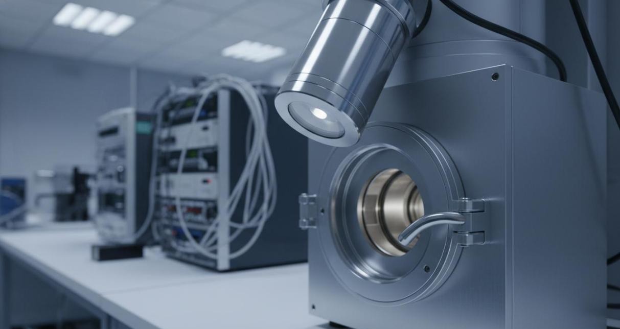 Figure 3: A silicon drift detector mounted on a scanning electron microscope for energy-dispersive X-ray spectroscopy.
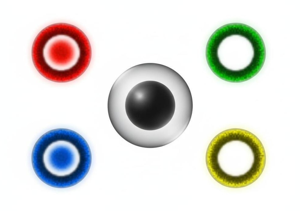 Figure 4: Color-coded EDS elemental maps of a core-shell nanoparticle showing the spatial distribution of multiple elements within the structure.
XPS and EDS: Complementary Techniques
While both techniques provide elemental information, XPS and EDS address fundamentally different analytical needs. Understanding their complementary strengths enables researchers to select the most appropriate technique or combine both for comprehensive characterization.
| Attribute | XPS | EDS |
| Probing depth | 1 to 10 nm (surface only) | 100 nm to several um |
| Chemical state | Yes, distinguishes bonding | No, elemental only |
| Spatial resolution | 10 to 100 um | Down to sub-nm (STEM) |
| Light elements | No H or He | No H, He, Li |
| Quantification | Atomic percent accurate | Semi-quantitative to quantitative |
| Mapping capability | Limited area mapping | High-resolution 2D mapping |
| Sample environment | Ultra-high vacuum required | Vacuum (SEM/TEM) |
| Depth profiling | Sputter and ARXPS available | Not typically available |
A common workflow at Eata Nanomaterials involves initial EDS screening to identify unexpected elements and assess overall composition, followed by targeted XPS analysis to determine chemical states, quantify functional group densities, and evaluate surface modification success.
XPS Depth Profiling for Layered and Core-Shell Structures
Many advanced nanomaterials feature intentionally engineered layered architectures: core-shell nanoparticles, multilayer thin films, gradient coatings, and surface-modified substrates. XPS depth profiling reveals how composition and chemistry evolve from the outermost surface through to the bulk.
We offer multiple depth profiling modalities tailored to different material systems:
Monatomic argon ion sputtering: The conventional approach using energetic Ar+ ions to sequentially remove material. Suitable for metals, oxides, and inorganic thin films. Careful parameter selection minimizes preferential sputtering artifacts and reduction of oxide species.
Gas cluster ion beam (GCIB) sputtering: Employing clusters of hundreds to thousands of argon atoms that distribute kinetic energy across a broader area, dramatically reducing chemical damage to organic and polymeric surfaces. Essential for analyzing soft matter coatings, biological functionalization layers, and OLED device structures.
Angle-resolved XPS: A non-destructive alternative for films thinner than the XPS sampling depth. By tilting the sample relative to the analyzer, the effective path length changes, probing shallower or deeper regions without material removal.
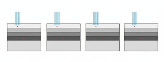 Figure 5: A schematic of XPS depth profiling showing sequential etching through a multilayer thin film structure with analysis at each step.
Applications in Nanomaterial Research
Our surface chemistry and composition analysis services support a broad spectrum of nanomaterial research programs:
- Verifying successful surface functionalization by detecting new elements and chemical states introduced during silanization, PEGylation, or bioconjugation reactions
- Confirming core-shell nanoparticle architectures through depth profiling and EDS elemental mapping showing distinct core and shell compositions
- Detecting surface contamination and trace impurities that may compromise nanomaterial performance or biocompatibility
- Characterizing oxide layers and passivation films on metal nanoparticles, quantifying thickness and oxidation state distributions
- Analyzing quantum dot shell composition, verifying stoichiometry and detecting shell defects that affect optical properties
- Evaluating catalyst surface composition after reaction cycles, identifying poisoning species and structural changes
- Assessing doping efficiency in doped metal oxide nanoparticles by quantifying dopant concentration at the surface versus bulk
Analysis Deliverables and Reporting
Every XPS and EDS analysis project includes a detailed report with the following components:
- High-resolution survey and detailed region spectra with peak assignments and binding energy references
- Quantitative elemental composition tables with atomic percentages and uncertainties
- Chemical state fitting results showing component peak positions, full width at half maximum values, and relative abundances
- Elemental maps and line scan profiles with clear visual presentation and quantitative annotations
- Depth profile plots showing elemental concentration versus etch time or depth for layered structures
- Expert interpretation discussing implications for your specific research application and recommendations for further analysis if warranted
Submit Your Samples for Surface Analysis
Whether you need to verify a surface functionalization, characterize a core-shell architecture, identify trace contaminants, or profile a multilayer coating, Eata Nanomaterials provides precise, actionable surface chemistry data backed by expert interpretation.
Contact our analytical team to discuss your sample type, surface chemistry questions, and recommended analysis plan. We will guide you through sample preparation requirements and provide a detailed quotation for your project.