

Nanoparticle Dispersion and Ink Formulation Services
Translating a bench-scale nanoparticle synthesis into a production-ready ink involves far more than simple dilution. A dispersion of silver nanoparticles that appears uniform in a small vial may clog an inkjet printhead within minutes if the particle size distribution contains tails above 200 nanometers. A carbon nanotube slurry with promising electrical properties may fail entirely in screen printing if its thixotropic recovery time exceeds the mesh release dynamics of the press. The gap between a functional nanomaterial and a printable formulation represents one of the most common bottlenecks in the development of flexible electronics, smart packaging, and optoelectronic devices.
Eata Nanomaterials bridges this gap through an integrated formulation pipeline that combines dispersion engineering, rheological optimization, and print-process validation. We start with commercially available or client-supplied nanoparticles and transform them into stable, printable inks validated against the specific deposition method and substrate intended for the end application.
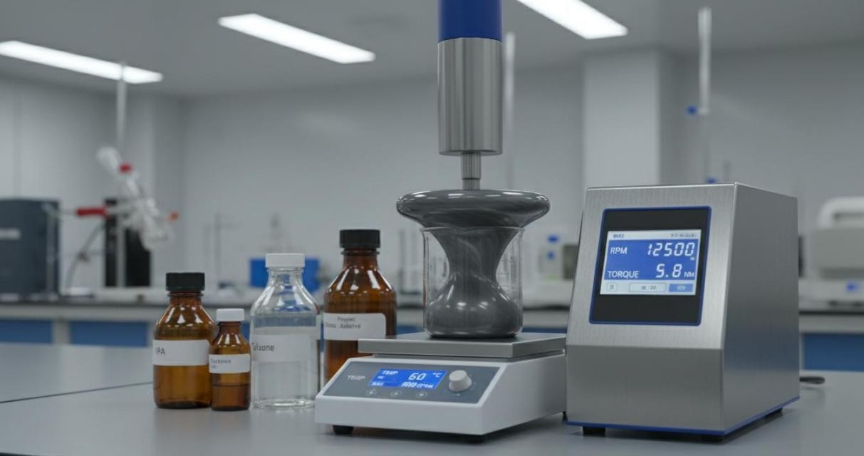 Figure 1: A high-shear dispersing homogenizer mixing silver nanoparticles into a polymer binder solution, with digital RPM and torque display for controlled dispersion processing.
Nanoparticle Dispersion Engineering
Stable nanoparticle dispersion is the foundation of every successful ink formulation. When nanoparticles are introduced into a liquid medium, they experience attractive van der Waals forces that drive aggregation unless counteracted by electrostatic or steric repulsion mechanisms. The selection and optimization of these stabilization strategies depend on the particle chemistry, the solvent system, and the processing conditions.
Our dispersion engineering services encompass:
- Electrostatic stabilization through pH adjustment and ionic dispersant selection, creating a surface charge layer that generates Coulombic repulsion between particles. This approach is effective in polar solvents and water-based systems where zeta potentials above 30 millivolts provide long-term colloidal stability
- Steric stabilization using polymeric dispersants such as polyvinylpyrrolidone, polyacrylic acid, or tailor-made block copolymers that adsorb onto particle surfaces and create a physical barrier preventing close particle approach. This method is preferred for non-polar solvents and high-solids-loadings where electrostatic repulsion is weakened
- Electrosteric stabilization combining both mechanisms, often achieved with polyelectrolyte dispersants that provide both charged groups for electrostatic repulsion and polymer chains for steric hindrance. This dual approach offers superior stability across broad pH and ionic strength ranges
- Dispersion equipment selection and parameter optimization including ultrasonic probe sonication, high-shear rotor-stator homogenization, bead milling, and three-roll milling. Each technique is matched to the particle toughness, desired fineness, and batch volume, with careful control of energy input to prevent particle fracture or amorphization of crystalline materials
Dispersion quality is verified through dynamic light scattering for hydrodynamic diameter and polydispersity index, zeta potential for surface charge characterization, and sedimentation analysis to predict shelf stability under storage and transport conditions.
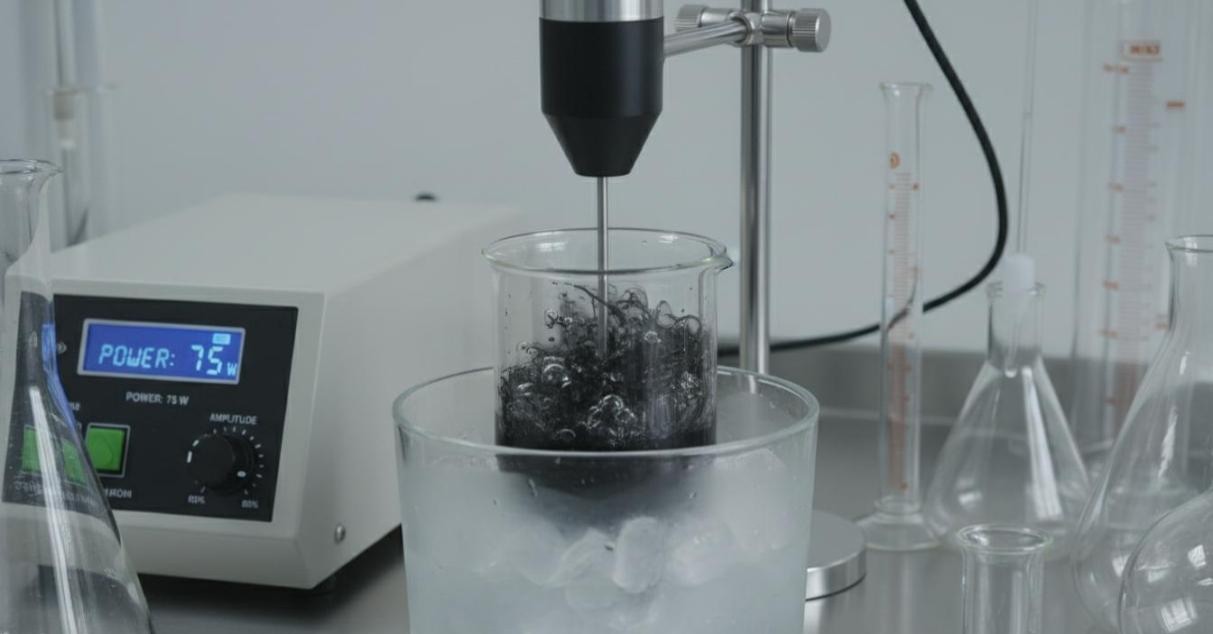 Figure 2: An ultrasonic probe sonicator dispersing carbon nanomaterials in a solvent within a beaker placed in an ice bath to prevent thermal degradation during high-energy processing.
Conductive Ink Formulation for Printed Electronics
Printed electronics fabrication places exacting demands on ink properties. The formulation must simultaneously provide sufficient conductivity after processing, maintain stability during storage, flow correctly through the deposition system, wet the substrate appropriately, and cure or sinter under conditions compatible with temperature-sensitive substrates such as PET or polyimide.
Our conductive ink formulation platform covers the full spectrum of functional nanomaterials:
- Silver nanoparticle inks optimized for inkjet, screen, and aerosol-jet printing with metal loadings from 10 to 60 weight percent. We select particle sizes between 5 and 50 nanometers for low-temperature sintering applications, and formulate with binder systems that balance adhesion and flexibility while maintaining sheet resistance below 50 milliohms per square after thermal or photonic sintering
- Carbon-based conductive inks incorporating carbon nanotubes, graphene, or carbon black for applications where cost, transparency, or oxidation resistance are priorities. We employ surfactant-assisted dispersion or polymer wrapping to achieve percolation thresholds as low as 0.1 weight percent for multi-walled carbon nanotubes in aqueous systems
- Copper and nickel nanoparticle inks as lower-cost alternatives to silver, formulated with antioxidant coatings and reductive sintering protocols to prevent oxide formation during processing. These systems achieve conductivity within a factor of two of silver at a fraction of the material cost
- Transparent conductive oxide inks including indium tin oxide, aluminum-doped zinc oxide, and antimony-doped tin oxide nanoparticles for optoelectronic applications requiring visible-light transparency combined with electrical conductivity
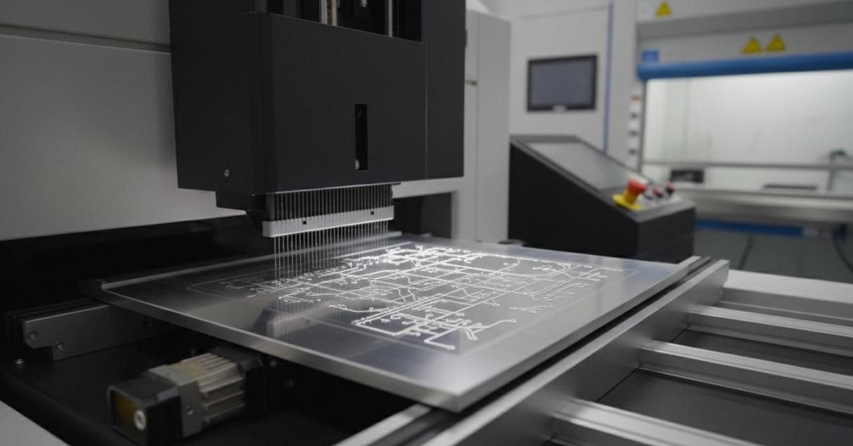 Figure 3: An inkjet printer depositing silver nanoparticle conductive ink onto a flexible PET substrate to form intricate circuit patterns with high spatial resolution.
Semiconductor and Dielectric Ink Development
Beyond conductive traces, functional printed electronics require semiconducting and insulating layers. We formulate these materials as printable inks compatible with the same deposition tools used for conductors, enabling multi-layer device fabrication without process switching.
Our semiconductor and dielectric ink portfolio includes:
- Perovskite quantum dot inks for light-emitting and photovoltaic applications. We formulate colloidal CsPbX3 quantum dot inks in non-polar aromatic solvents with viscosity and surface tension tuned for inkjet and electrohydrodynamic printing. Additives such as polyvinylpyrrolidone are incorporated to suppress coffee-ring effects and achieve uniform film formation
- Organic semiconductor inks based on small molecules and conjugated polymers dissolved or dispersed in halogenated or non-halogenated solvents. We employ Hansen solubility parameter analysis to identify optimal solvent blends that maximize solubility while controlling evaporation rate and film morphology
- Dielectric inks formulated from barium titanate, alumina, or polymer-ceramic composites for capacitor and transistor gate dielectric applications. These inks are optimized for high solids loading with controlled viscosity to produce dense, crack-free films after curing
- Photoluminescent inks containing quantum dots or phosphor particles for display backlighting and security applications, formulated with UV-curable binders for rapid patterning and encapsulation
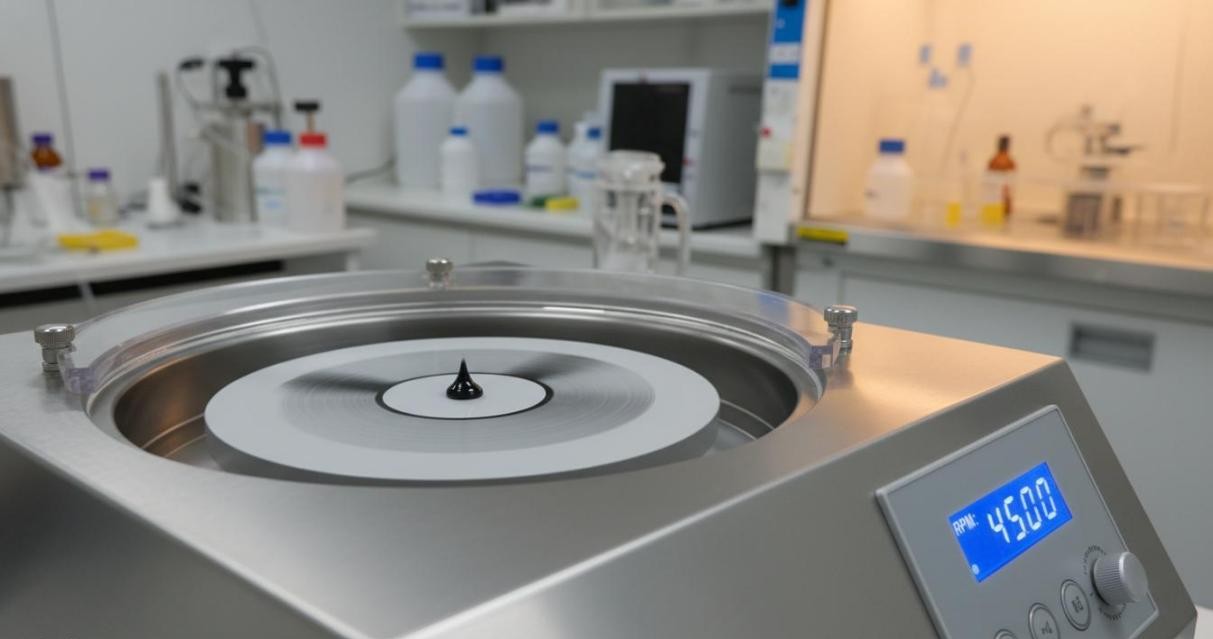 Figure 4: A spin coater spreading a droplet of quantum dot ink across a substrate surface at high rotational speed for uniform thin-film deposition.
Rheological Optimization for Print Processes
Each printing technology imposes distinct rheological requirements. An ink that flows perfectly through an inkjet nozzle will likely bleed uncontrollably in screen printing, while a screen-printable paste will almost certainly clog microfluidic inkjet channels. Our formulation process tailors viscosity, surface tension, and viscoelastic response to the specific printing method.
Process-specific formulation targets:
- Inkjet printing: viscosity between 2 and 20 millipascal-seconds at shear rates of 10,000 to 100,000 per second, surface tension between 20 and 50 millinewtons per meter for reliable droplet formation, and particle sizes below 200 nanometers to prevent nozzle clogging. We optimize these parameters using Ohnesorge number analysis to ensure clean droplet ejection without satellite formation
- Screen printing: viscosity between 1 and 50 pascal-seconds at low shear with pronounced shear-thinning behavior and rapid thixotropic recovery. These properties ensure the ink flows through the mesh under squeegee pressure yet maintains pattern definition after snap-off. Yield stress values above 10 pascals prevent post-print sagging and spreading
- Spin coating: viscosity between 5 and 50 millipascal-seconds with Newtonian or mildly shear-thinning behavior, optimized for substrate rotational speeds between 500 and 6,000 RPM to achieve target film thicknesses from 10 nanometers to 10 micrometers
- Roll-to-roll gravure and flexographic printing: viscosity and surface tension matched to the cell geometry and doctor blade system of the press, with fast-drying solvent systems enabling high-speed coating at web speeds above 10 meters per minute
Ink Composition and Formulation Parameters
| Ink Type | Conductive Filler | Loading | Post-Process Rs | Sintering Method |
| Ag NP inkjet | Ag nanoparticles (5-50nm) | 10-30 wt% | 5-50 mOhm/sq | Thermal 120-250C |
| Ag NP screen | Ag nanoparticles (20-100nm) | 40-60 wt% | <10 mOhm/sq | Thermal or IPL |
| CNT ink | Multi-walled CNTs | 0.1-5 wt% | 100-1000 Ohm/sq | 100-150C cure |
| Graphene ink | Few-layer graphene | 1-10 wt% | 50-500 Ohm/sq | Thermal or laser |
| Cu alloy ink | Cu or Cu-Ag core-shell | 30-50 wt% | 20-100 mOhm/sq | Reductive atmosphere |
| Perovskite QD | CsPbX3 quantum dots | 5-20 wt% | N/A | Room temp drying |
Sintering and Post-Processing Optimization
After deposition, the printed pattern must be converted from a dispersion of discrete nanoparticles into a continuous functional layer. This transformation requires removal of solvents and dispersants followed by neck formation and grain growth between particles. Eata Nanomaterials develops sintering protocols matched to the substrate thermal budget and production throughput requirements:
- Thermal sintering in convection or infrared ovens with precisely controlled temperature ramps and dwell times, suitable for substrates tolerant of 120 to 250 degrees Celsius exposure. Ramp rates of 5 to 10 degrees per minute prevent substrate warping and solvent blistering
- Photonic sintering using intense pulsed light or continuous-wave laser exposure, enabling millisecond-scale processing of heat-sensitive substrates such as PET and paper. Pulse energy and duration are optimized to drive nanoparticle coalescence without damaging the underlying substrate
- Plasma sintering using argon or hydrogen plasma to remove organic ligands and promote surface atomic diffusion at temperatures below 100 degrees Celsius, ideal for ultra-thin flexible substrates and textile materials
- Chemical sintering using formic acid vapor or chloride salts to remove stabilizing ligands and initiate particle fusion at reduced temperatures, particularly effective for copper and nickel nanoparticle systems prone to oxidation during thermal processing
Each sintering protocol is validated through four-point probe sheet resistance measurement, scanning electron microscopy of film morphology, and adhesion testing by tape peel and bend testing to ensure the printed layer survives subsequent processing and end-use mechanical stress.
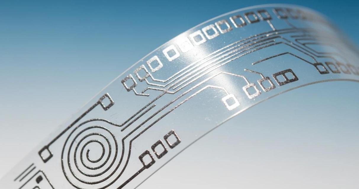 Figure 5: A flexible printed circuit fabricated with silver nanoparticle conductive ink on a transparent PET substrate, demonstrating fine conductive traces and an antenna spiral pattern.
Application Areas
Our nanoparticle dispersion and ink formulation services support diverse research and development programs:
- Flexible printed circuit boards and interconnects for wearable electronics, where silver nanoparticle inks on polyimide substrates provide bendable conductive traces with mechanical durability exceeding 10,000 flex cycles
- RFID antennas and NFC tags for smart packaging and logistics, where screen-printed silver or copper inks on paper substrates offer a cost-effective alternative to etched metal antennas
- Biosensor electrodes for glucose monitoring and electrochemical diagnostics, where carbon or gold nanoparticle inks provide high surface area, biocompatible interfaces for enzyme immobilization and signal transduction
- Transparent heaters and defrosters for automotive and aerospace applications, where silver nanowire or carbon nanotube inks balance optical transparency above 85 percent with sheet resistance below 100 ohms per square
- Quantum dot color conversion layers for micro-LED displays, where inkjet-printed perovskite quantum dot arrays achieve sub-10-micrometer pixel dimensions with photoluminescence quantum yields exceeding 90 percent
Sample Submission and Collaboration
Clients may supply their own nanoparticles or request sourcing through our established network of nanoparticle manufacturers. For custom formulation projects, we typically require 1 to 10 grams of nanopowder or 10 to 100 milliliters of nanoparticle dispersion as starting material. Detailed information about particle composition, surface chemistry, and intended application accelerates the formulation optimization process.
For clients starting from scratch, we offer integrated packages encompassing nanoparticle synthesis, dispersion preparation, ink formulation, and print validation. All formulations are documented with complete compositional data, processing parameters, and characterization results, ensuring reproducibility and enabling seamless technology transfer to manufacturing partners.
If you are interested in our products or services, please don't hesitate to contact us.