

Electrical Conductivity and Carrier Mobility Testing Services
Electrical transport properties form the foundation of virtually every functional application of nanomaterials. From transparent conductive electrodes to quantum dot photovoltaics, battery anode materials to flexible printed electronics, the ability to move charge efficiently through or across nanostructured materials determines performance at the most fundamental level. Characterizing these properties requires precise measurement techniques that account for the unique challenges posed by nanoscale dimensions, high surface-to-volume ratios, and often non-ideal contact geometries.
At Eata Nanomaterials, our electrical characterization laboratory is equipped with a multi-technique platform spanning direct current, alternating current, and magnetic-field-assisted measurements. We provide comprehensive electrical testing services for conductive nanoparticles, semiconductor nanocrystals, nanowire networks, thin films, and nanocomposite materials, delivering quantitative data that links nanostructure to electronic function.
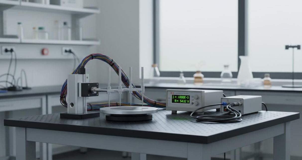 Figure 1: A four-point probe resistivity measurement station with probe head and source meter on an optical table.
Four-Point Probe Resistivity and Sheet Resistance
The four-point probe method represents the industry standard for measuring the resistivity and sheet resistance of thin conductive films and pressed powder samples. By using four collinear electrodes with the outer two sourcing current and the inner two sensing voltage, this geometry eliminates contact resistance contributions that plague two-terminal measurements, providing accurate determination of intrinsic material resistivity.
Our four-point probe services cover:
- Sheet resistance (Rs) measurement of thin films and coatings deposited on insulating substrates, with results reported in ohms per square
- Bulk resistivity of powder compacts and sintered pellets using the van der Pauw geometry for isotropic materials and rectangular bar configurations for anisotropic samples
- Film thickness-normalized conductivity calculation when thickness data is provided, converting sheet resistance to volumetric conductivity
- Temperature-dependent resistivity profiling from room temperature to 300 degrees Celsius, revealing metallic versus semiconducting transport behavior through resistance temperature coefficients
- Line mapping across wafer-scale samples to assess deposition uniformity and identify spatial variation in resistivity
For nanomaterial films deposited from colloidal inks, we offer specialized protocols that account for percolation thresholds, grain boundary resistance, and porosity effects that strongly influence measured conductivity relative to bulk crystalline values.
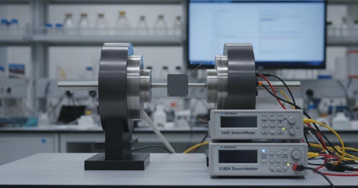 Figure 2: A Hall effect measurement system with sample inside a cryostat between electromagnet pole pieces and source meter instruments.
Hall Effect Measurement for Carrier Type, Density, and Mobility
The Hall effect provides the most direct and widely accepted method for determining the fundamental electronic parameters of a semiconductor: carrier type (electron or hole), carrier concentration, and carrier mobility. When a magnetic field is applied perpendicular to a current-carrying sample, the Lorentz force deflects charge carriers to one side, creating a measurable transverse voltage known as the Hall voltage.
Our Hall effect measurement services deliver:
- Carrier type determination identifying whether electrons or holes dominate transport, critical for understanding doping efficiency in semiconductor nanocrystals
- Carrier concentration quantifying the number density of free charge carriers per cubic centimeter, from degenerate levels above 10^20 cm^-3 to lightly doped regimes below 10^14 cm^-3
- Hall mobility calculated from the ratio of conductivity to carrier concentration, representing the average drift velocity per unit electric field and serving as the key figure of merit for transistor channel materials
- Temperature-dependent Hall measurements from 77 K to 500 K revealing activation energies of dopants, identifying impurity band conduction, and detecting metal-insulator transitions
- Variable magnetic field sweeps enabling multi-carrier analysis through magnetic field-dependent conductivity tensor fitting for samples with mixed electron and hole conduction
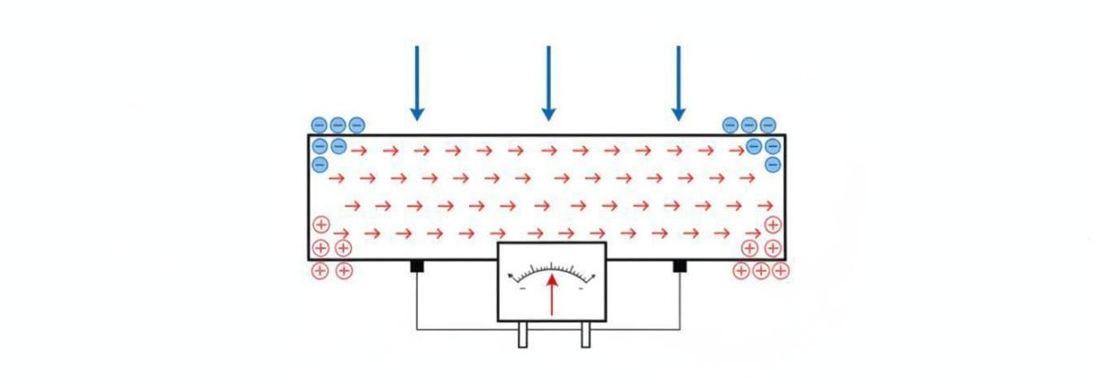 Figure 3: A schematic of the Hall effect showing charge carrier deflection by a perpendicular magnetic field and resulting Hall voltage.
Current-Voltage Characterization and Device Testing
Current-voltage characterization provides fundamental insight into the conduction mechanisms, contact quality, and device-relevant performance of nanomaterial-based structures. Our precision source-measure unit enables highly sensitive I-V measurements spanning femtoampere to ampere current ranges with microvolt resolution.
We offer the following I-V measurement capabilities:
- Two-point and four-point I-V sweeps identifying ohmic versus Schottky contact behavior and quantifying contact resistance contributions
- Thin film transistor transfer and output characteristics for nanomaterial-based field-effect devices, extracting field-effect mobility, threshold voltage, on-off ratio, and subthreshold swing
- Photoconductivity measurements under controlled illumination intensities and wavelengths, determining responsivity and gain of nanomaterial photodetectors
- Cyclic voltammetry and chronoamperometry for battery electrode materials, evaluating charge capacity, rate capability, and Coulombic efficiency
- Gate-dependent conductivity measurements revealing the influence of electrostatic doping on carrier density and transport in 2D material devices
 Figure 4: An I-V characteristic curve showing the nonlinear current-voltage response of a semiconductor nanomaterial thin film.
Electrochemical Impedance Spectroscopy
Electrochemical impedance spectroscopy measures the resistance and capacitance of electrochemical systems across a wide frequency range. For nanomaterial researchers, EIS provides unique insights into ion transport through porous electrodes, charge transfer at nanoparticle-electrolyte interfaces, and the double-layer capacitance of high-surface-area nanostructures.
Our EIS analysis services include:
- Nyquist and Bode plot acquisition and equivalent circuit fitting, extracting solution resistance, charge transfer resistance, Warburg impedance, and double-layer capacitance
- Ionic conductivity measurement of solid electrolytes and gel polymer electrolytes containing ceramic nanofiller dispersions
- Interfacial impedance analysis quantifying the resistance and capacitance at nanoparticle-electrode boundaries in composite battery electrodes
- Frequency-dependent capacitance determination for supercapacitor electrodes, evaluating the contribution of electric double-layer versus pseudocapacitive charge storage mechanisms
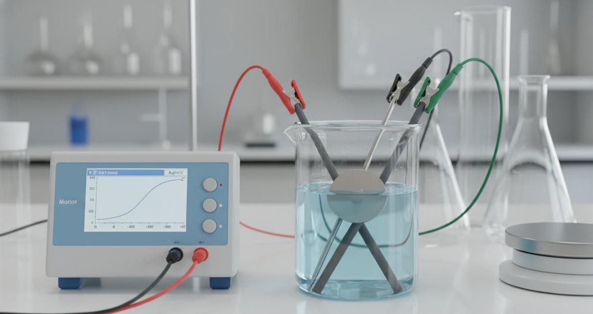 Figure 5: A three-electrode electrochemical cell connected to a potentiostat for impedance spectroscopy measurements.
Technique Selection Guide
| Measurement Need | Recommended Technique | Output Parameters |
| Film or pellet resistivity | Four-point probe | Resistivity, sheet resistance |
| Carrier type, density, mobility | Hall effect | n or p, concentration, mobility |
| Contact quality, device I-V | Two/four-point I-V | Resistance, ideality factor |
| Transistor performance | FET characterization | Mobility, Vth, on-off ratio |
| Electrode interfacial properties | EIS | Rct, Cdl, ionic conductivity |
| Photoresponse quantification | Photoconductivity I-V | Responsivity, gain |
| Temperature-dependent transport | Variable T four-point / Hall | Activation energy, TCR |
Applications Across Nanomaterial Research
Our electrical characterization services support a diverse range of nanomaterial research programs:
- Transparent conductive films evaluating the trade-off between sheet resistance and optical transparency for indium tin oxide alternatives based on silver nanowires, carbon nanotubes, or graphene
- Semiconductor nanocrystal inks assessing carrier mobility in field-effect transistor channels for printed electronics applications
- Battery electrode materials measuring electronic conductivity and interfacial impedance to identify rate-limiting steps in charge storage
- Perovskite solar cells characterizing ion migration and hysteresis through frequency-dependent impedance analysis
- 2D material devices extracting mobility from gate-dependent conductivity in transition metal dichalcogenide transistors
- Conductive polymer nanocomposites establishing percolation thresholds and optimizing filler loading for antistatic and electromagnetic shielding applications
Measurement Deliverables
Every electrical characterization project includes a comprehensive report containing:
- Raw and processed measurement data in standard formats for independent analysis or archival
- Extracted parameters with calculated uncertainties, including resistivity, carrier concentration, mobility, and derived figures of merit
- Publication-quality figures showing I-V curves, Hall voltage data, Nyquist plots, or temperature-dependent conductivity as appropriate
- Experimental conditions documenting measurement geometry, applied fields, temperature, and sample preparation details
- Expert interpretation discussing transport mechanisms, contact effects, and recommendations for material or device optimization
Submit Your Samples for Electrical Characterization
Whether you need to verify the conductivity of a transparent electrode, quantify carrier mobility in a semiconductor nanocrystal ink, or dissect interfacial impedance in a battery electrode, Eata Nanomaterials provides precise, reliable electrical characterization with expert interpretation tailored to your research objectives.
Contact our analytical team to discuss your sample type, desired measurements, and electrode configuration requirements. We will recommend the optimal techniques and provide guidance on sample preparation and geometry.