

Perovskite Nanocrystal Synthesis Services
Metal halide perovskite nanocrystals have fundamentally redefined what is achievable in solution-processed optoelectronics. These colloidal semiconductor nanocrystals, most commonly formulated as CsPbX3 where X represents chlorine, bromine, iodine, or mixtures thereof, exhibit photoluminescence quantum yields approaching unity, emission linewidths as narrow as 8-40 nm full width at half maximum, and bandgap tunability spanning the entire visible spectrum through simple halide composition adjustment. Since the landmark report by Protesescu et al. in 2015, perovskite nanocrystals have matured from a laboratory curiosity into a serious contender for next-generation displays, lighting systems, lasers, and photodetectors.
At Eata Nanomaterials, we have developed a comprehensive perovskite nanocrystal synthesis platform that delivers colloidal nanocrystals with precisely engineered optical properties, exceptional crystallinity, and operational stability. Our capabilities span the two dominant synthetic routes — hot-injection and room-temperature ligand-assisted reprecipitation — and extend through halide anion exchange, surface passivation engineering, shape control, and protective encapsulation. Whether your project demands high-purity RGB emitters for quantum-dot LEDs or stabilized nanocrystals for bioconjugation, we provide materials that meet your exact specifications.
Hot-Injection & Room-Temperature Synthesis Routes
 Figure 1: CsPbBr3 perovskite nanocrystals with cubic morphology exhibiting characteristic bright green photoluminescence
The synthesis of high-quality perovskite nanocrystals demands precise control over precursor chemistry, ligand identity, reaction temperature, and quenching kinetics. We offer both the hot-injection method, which produces nanocrystals with the highest crystallinity and quantum yields, and the room-temperature reprecipitation method, which offers simplified processing and scalability advantages. The choice of route depends on the target composition, desired particle size, and specific application requirements.
In the hot-injection approach, a cesium oleate precursor is rapidly injected into a hot solution of lead halide and surface ligands in octadecene. The sudden supersaturation triggers burst nucleation followed by rapid growth, yielding monodisperse nanocubes within seconds. Temperature control is critical — the injection temperature determines nanocrystal size, while the ligand ratio influences morphology and colloidal stability. Our optimized protocols achieve near-unity quantum yields for green-emitting CsPbBr3 by carefully balancing oleylamine and oleic acid concentrations.
The room-temperature reprecipitation method provides an attractive alternative for compositions sensitive to thermal degradation. A polar precursor solution containing cesium and lead salts is injected into a non-polar antisolvent, inducing rapid crystallization at ambient temperature. This approach is particularly valuable for chloride-rich compositions and mixed-halide systems where thermal processing can induce phase segregation.
Synthesis capabilities:
- Hot-injection synthesis: CsPbCl3, CsPbBr3, CsPbI3 and mixed-halide CsPb(Cl/Br/I)3; injection temperatures 140-200 C; QY up to 95% for CsPbBr3; sizes 4-15 nm.
- Room-temperature reprecipitation: All CsPbX3 compositions; scalable batch processing; spherical quantum dots and nanocubes; ideal for halide-sensitive formulations.
- Formamidinium perovskites: FAPbBr3 and FAPbI3 with enhanced thermal stability; low-temperature nanowire growth; red-shifted emission compared to cesium analogues.
- Double perovskites: Lead-free Cs2AgBiBr6 and related compositions; reduced toxicity for environmentally sensitive applications.
- Precursor optimization: Cesium oleate with controlled Cs:OA ratios for complete conversion and reproducibility; moisture-free Schlenk-line and glovebox processing.
Composition-Tuned Emission Across the Visible Spectrum
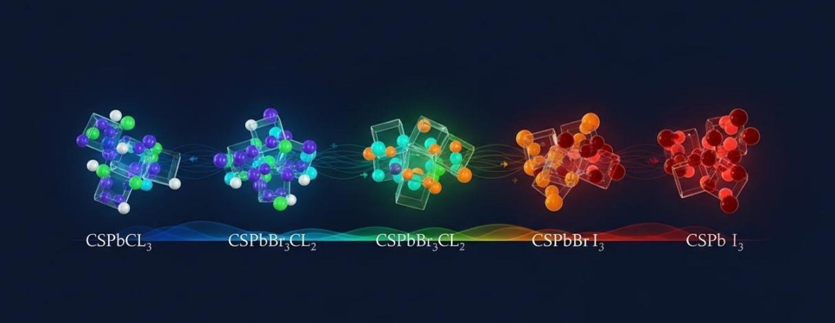 Figure 2: Halide anion exchange in perovskite nanocrystals enabling continuous emission tuning from blue through green to red
One of the most powerful features of halide perovskite nanocrystals is the ability to tune emission wavelength across the entire visible spectrum through halide composition rather than quantum confinement. In CsPbX3, replacing chloride with bromide and subsequently iodide progressively red-shifts the bandgap from 3.0 eV to 1.7 eV, corresponding to emission from deep blue at 410 nm to near-infrared at 700 nm. This composition-tunability enables access to pure, saturated RGB colors that exceed the performance requirements of next-generation wide-gamut displays.
We achieve precise emission control through two complementary strategies. Direct synthesis using predetermined halide precursor ratios produces nanocrystals with target compositions and emission wavelengths. Alternatively, post-synthetic halide anion exchange enables fine-tuning of emission without changing nanocrystal size — a uniquely powerful capability of the perovskite system. The anion exchange reaction proceeds rapidly at room temperature through addition of excess halide salt, enabling systematic exploration of the full compositional space.
| Composition | Emission Peak | Color | Application |
| CsPbCl3 | 400-420 nm | Deep Blue | Blue LED emitters, UV photocatalysts |
| CsPb(Cl/Br)3 | 420-510 nm | Sky Blue to Cyan | Display blue pixels, lighting |
| CsPbBr3 | 510-530 nm | Green | Display green pixels, lasers |
| CsPb(Br/I)3 | 530-630 nm | Yellow to Orange | Amber LEDs, signaling |
| CsPbI3 | 630-700 nm | Red to Deep Red | Display red pixels, NIR applications |
Shape-Controlled Nanocrystal Morphology
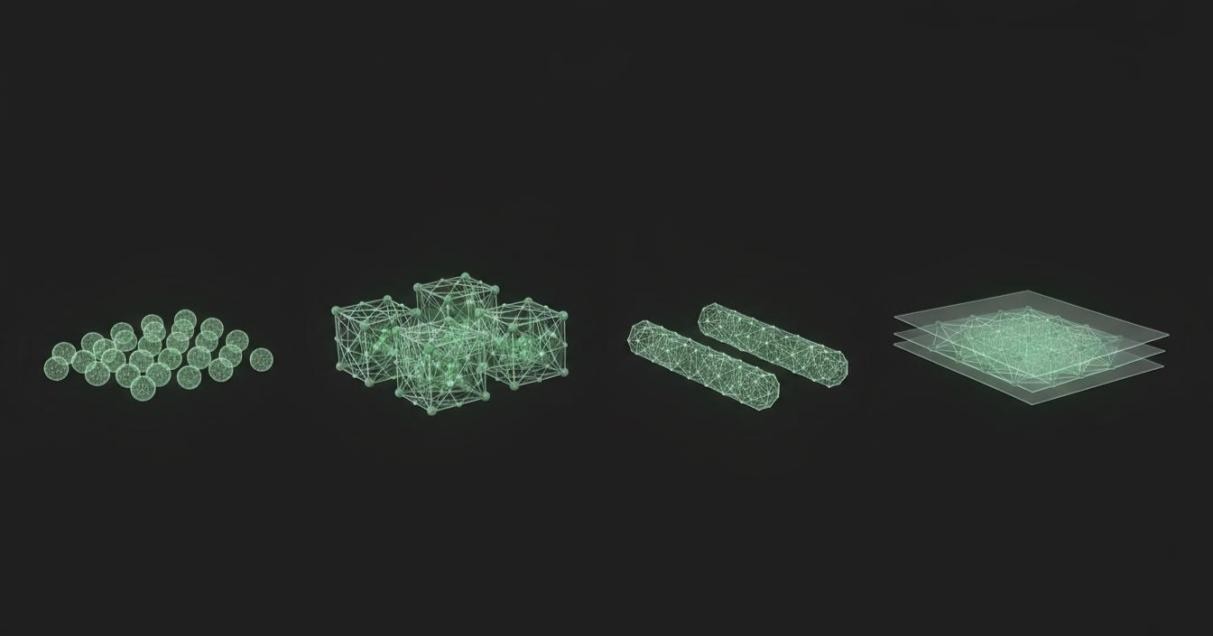 Figure 3: Shape-controlled perovskite nanocrystals including spherical quantum dots, nanocubes, nanorods, and nanoplatelets
Beyond the standard cubic morphology, perovskite nanocrystals can be engineered into a variety of shapes with dimensionality-dependent optical and electronic properties. Zero-dimensional quantum dots exhibit the highest quantum yields and photostability. One-dimensional nanowires function as natural optical cavities for lasing. Two-dimensional nanoplatelets display exceptionally narrow emission linewidths due to strong quantum confinement in one dimension. Our shape control service leverages ligand-mediated synthesis strategies to produce perovskite nanocrystals with precisely defined morphologies.
The key to shape control lies in the identity and ratio of the organic ligands used during synthesis. Long-chain alkylammonium halides preferentially bind to specific crystallographic facets, directing anisotropic growth. Higher concentrations of amine ligands favor nanorod and nanowire formation, while acid-rich conditions promote the formation of nanocubes and spherical dots. The reaction temperature also plays a critical role — lower temperatures favor kinetic control and anisotropic shapes, while higher temperatures produce more isotropic morphologies under thermodynamic control.
Shape catalog:
- Nanocubes (0D): Isotropic emission; highest QY; standard morphology for display and LED applications; sizes 4-15 nm.
- Nanorods & nanowires (1D): Natural optical cavities for lasing; polarized emission; length 100 nm to several microns; diameter 5-20 nm.
- Nanoplatelets (2D): Ultra-narrow FWHM 8-20 nm; strong quantum confinement in thickness direction; thickness 1-5 unit cells.
- Hierarchical architectures: Self-assembled superlattices and microcrystals; enhanced light outcoupling for LED applications.
Surface Passivation & Stability Enhancement
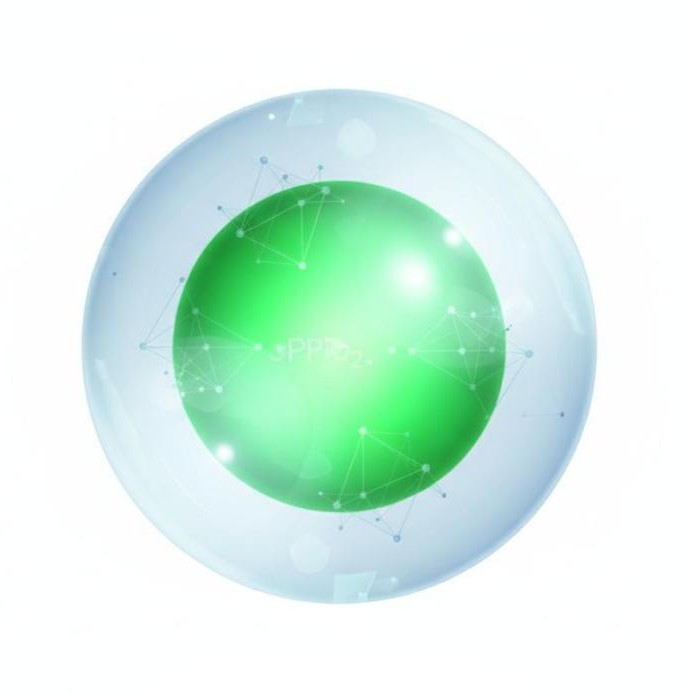 Figure 4: Core-shell perovskite nanocrystal with CsPbBr3 core encapsulated within a protective silica shell for enhanced stability
The operational stability of perovskite nanocrystals remains the primary barrier to widespread commercial adoption. These materials are inherently sensitive to moisture, polar solvents, oxygen, elevated temperatures, and prolonged UV illumination. At Eata Nanomaterials, we have developed a comprehensive stability enhancement portfolio that addresses each of these vulnerability points through surface chemistry engineering, protective encapsulation, and composite formulation strategies.
Surface passivation targets the root cause of instability — the dynamic, easily detached ligand shell that leaves lead-rich surface sites exposed to chemical attack. We employ L-type ligand strategies using primary amines that bind more strongly to surface lead atoms than conventional X-type oleic acid-oleylamine pairs. Lead halide-rich surface treatment heals trap states and restores quantum yield. For long-term stability, encapsulation within inorganic matrices provides a hermetic barrier against environmental degradation.
- L-type ligand passivation: Primary amine-only capping (n-octylamine, oleylamine) without oleic acid; eliminates proton exchange-induced ligand detachment; QY approaching 100% for CsPbBr3.
- Lead halide surface treatment: Post-synthetic treatment with PbBr2 or halide salts; heals surface vacancies and non-radiative trap states; restores and enhances photoluminescence.
- Silica encapsulation: Stober-type sol-gel coating of individual nanocrystals; protects against moisture and oxygen; maintains colloidal dispersibility.
- Polymer matrix embedding: Incorporation into PMMA, PS, or PVP matrices; dramatically improved moisture resistance and thermal stability for film applications.
- Core-shell architectures: Oxide and lead halide overcoating; type-I band alignment for electronic confinement and surface protection.
Perovskite Nanocrystal Film & LED Device Processing
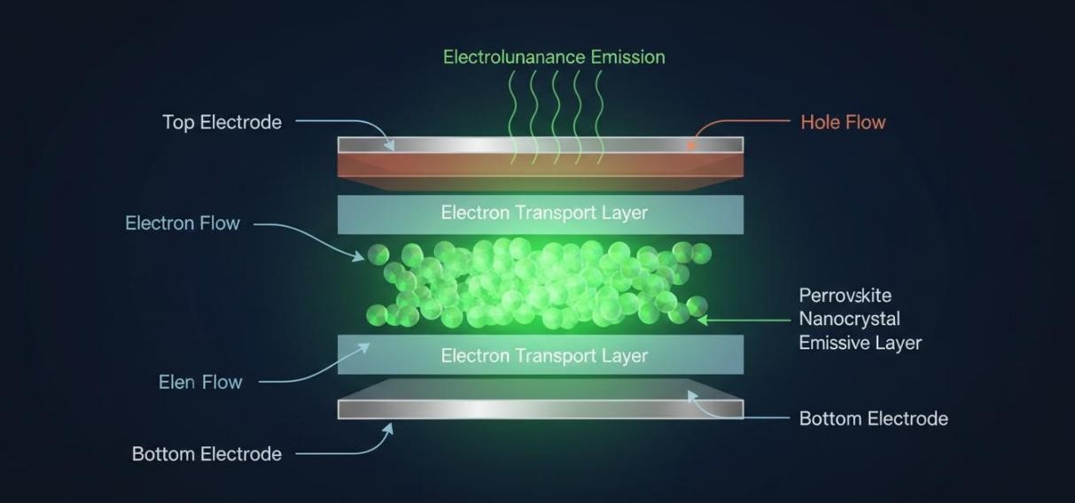 Figure 5: Layered perovskite nanocrystal LED device architecture showing electron transport layer, emissive perovskite layer, and hole transport layer
The exceptional optical properties of perovskite nanocrystals translate into extraordinary device performance in light-emitting diode architectures. PeLED external quantum efficiencies have surged from below 1% in 2015 to over 25% today, rivaling the performance of commercial OLEDs and quantum dot LEDs. Key to this progress has been the development of nanocrystal inks that can be deposited into uniform, pinhole-free films compatible with solution-processed charge transport layers.
Our perovskite LED device processing service supports clients in translating high-quality nanocrystals into functioning prototype devices. We optimize nanocrystal ink formulations for spin-coating and inkjet printing, engineer ligand exchange protocols for enhanced charge injection, and assist in the selection and deposition of compatible electron and hole transport layers. The result is a complete materials stack optimized for maximum luminance, efficiency, and operational lifetime.
LED processing capabilities:
- Nanocrystal ink formulation: Concentrated colloidal inks in non-polar solvents; optimized for spin-coating, blade-coating, and inkjet printing; stable against aggregation.
- Short-ligand exchange: Replacement of long-chain oleic acid/oleylamine with short aromatic ligands (4-bromobenzylphosphonic acid) for enhanced charge transport.
- Device stack consultation: Selection of ZnO, TiO2, or SnO2 electron transport layers; TFB, poly-TPD, or CBP hole transport layers; ITO and FTO transparent electrode compatibility.
- Film optimization: Concentration tuning, anti-solvent treatment, and annealing protocols for uniform, pinhole-free nanocrystal films with high photoluminescence.
Comprehensive Photophysical Characterization
Every batch of perovskite nanocrystals undergoes rigorous photophysical and structural characterization to confirm emission wavelength, quantum yield, size distribution, crystallinity, and colloidal stability. Our characterization reports provide the complete data package needed for research publication, process transfer, and quality control.
- Optical spectroscopy: UV-Vis absorption and steady-state photoluminescence spectroscopy for peak position, FWHM, and Stokes shift; absolute quantum yield measurement via integrating sphere.
- Structural analysis: Powder X-ray diffraction for phase purity and crystallite size; transmission electron microscopy for morphology and size distribution.
- Time-resolved spectroscopy: Time-correlated single photon counting for exciton lifetime measurement; identification of radiative and non-radiative recombination pathways.
- Colloidal stability: Dynamic light scattering for hydrodynamic size; zeta potential for surface charge; long-term storage monitoring under ambient and elevated temperature conditions.
- Stability assessment: Photostability testing under continuous UV excitation; moisture resistance evaluation; thermal cycling studies.
Illuminate Your Next Display Technology with Precision-Engineered Perovskite Nanocrystals
Get in touch with Eata Nanomaterials to discuss your perovskite nanocrystal synthesis requirements. Our materials scientists will develop a tailored formulation with precisely tuned emission, optimized stability, and surface chemistry matched to your device or application platform.