

Products
- High-Quality Graphene
- CVD Graphene, Graphene-Like Materials
- Graphene-Like Series
- Defect-Free Single-Crystal Graphene and Graphene-Like Materials (Mechanical Exfoliation)
- Quantum Dot Series
- Aggregation-Induced Emission (AIE)
- Near-Infrared II (NIR-II) Fluorescent Dyes
- Graphdiyne
- Two-Dimensional Transition Metal Carbides/Nitrides/Borides (MXene)
- Metal Nanomaterials and Other Functional Bio-Nanomaterials
- Metal-Organic Frameworks (MOF)
- Covalent Organic Frameworks (COF)
- Two-Dimensional Layered Metal Oxides (LDH)
- Carbon Nanotube Powders, Pastes
- Carbon Nanotube Arrays and Special Carbon Nanotube Materials
- High-Quality Metallic and Semiconducting High-Purity Single-Walled Carbon Nanotubes
- Carbon Nanotube Sponges
- Mesoporous Carbon and Carbon Nanomaterials
- High-Quality Fullerenes
- One-Dimensional Nanomaterials
- Molecular Sieves
- Inorganic Nanomaterials
- Perovskite Materials
- Highly Oriented Pyrolytic Graphite (HOPG)
- Organic Materials
- Single-Atom Catalysts
- Thermoelectric Materials
- Sodium Storage Materials
- Industrial-Grade Nanomaterials
- Solid-State Lithium Batteries
- Hydrogel Series and Consumables
Online Inquiry
Graphene-Like Series
A Whole Family of Atomically Thin Materials Awaits
When graphene burst onto the scene in 2004, it opened a door that scientists had suspected existed but never quite managed to unlock: the world of two-dimensional materials. Today, the landscape looks dramatically different. Researchers no longer ask simply whether a material can be thinned down to a single layer. Instead, they mix and match an ever-growing catalog of graphene-like substances, stacking them into van der Waals heterostructures that behave unlike anything found in nature. Eata Nanomaterials supplies this expanding family of layered solids — from insulating hexagonal boron nitride to semiconducting transition metal dichalcogenides, from metallic MXenes to anisotropic black phosphorus — each produced with the reproducibility and characterization rigor that serious science demands.
The unifying thread among these materials is their crystal architecture: strong covalent bonds hold atoms together within each plane, while weak van der Waals forces let adjacent planes slide apart. That structural duality makes exfoliation possible, whether by adhesive tape, ultrasonic bombardment in solvent, or chemical intercalation. It also means that layer count becomes a continuously tunable knob, letting engineers dial in electronic and optical properties that shift predictably from bulk to monolayer limits. Our Graphene-Like Series covers the full spectrum of these layered solids, ready for integration into your next device, composite, or catalytic platform.
Featured Products
| Material | High-Volume Search Specs | Where It Gets Used |
| h-BN | Monolayer hBN, CVD hBN on Cu, dielectric substrate, van der Waals heterostructure substrate, flatness <0.15 nm | Graphene encapsulation, tunnel barrier, UV emitter, 2D FET dielectric |
| MoS2 | Monolayer MoS2, 1.8 eV direct bandgap, CVD grown, 2H phase, PL peak 1.9 eV, n-type FET channel | Transistors, photodetectors, catalysis H2 evolution, flexible optoelectronics |
| WS2 | Monolayer WS2, valley polarization, strong spin-orbit coupling, CVD on sapphire, PL quantum yield | Valleytronics devices, spintronic components, photoluminescent sensors |
| WSe2 | Monolayer WSe2, ambipolar transport, p-type 2D semiconductor, CVD grown, field-effect mobility | Complementary logic with MoS2, infrared detectors, heterostructure diodes |
| MoSe2 | Monolayer MoSe2, higher electron mobility than MoS2, infrared absorption, direct gap semiconductor | High-frequency FETs, near-infrared photovoltaics, quantum dot integration |
| MXene Ti3C2Tx | Ti3C2Tx MXene delaminated, aqueous dispersion, metallic conductivity 8000 S/cm, HF etched, clay form | EMI shielding, supercapacitor electrode, battery anode, conductive ink, sensor |
| Ti2CTx MXene | Ti2CTx MXene, lighter than Ti3C2Tx, larger interlayer spacing, Li-ion intercalation | Energy storage, lightweight composite filler, electrochemical actuator |
| Black Phosphorus | Few-layer phosphorene, bandgap 0.3-2.0 eV, anisotropic mobility, hBN encapsulated, stable FET | Mid-IR photodetector, anisotropic electronic device, fast-switching transistor |
| Graphene Oxide | Single-layer GO, Hummers method, 1-20 um flake size, dispersible in water, C/O ratio 2-4 | Membrane separation, composite precursor, drug carrier, reduction to rGO |
| rGO | Reduced graphene oxide, hydrazine or thermal reduction, C/O >10, conductive powder or film | Battery electrode, supercapacitor, EMI shielding, conductive coating |
Meet the Members of Our Graphene-Like Series
h-BN: The Quiet Workhorse of 2D Electronics
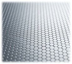
Hexagonal boron nitride does not grab headlines the way graphene does. That is a shame, because almost every high-performance graphene device ever built owes something to h-BN. With an atomically flat surface, a wide bandgap near 6 eV, and exceptional thermal stability, h-BN serves as the ideal substrate and gate dielectric for van der Waals heterostructures. Our CVD-grown h-BN films on copper foil can be transferred onto your target wafer with the same wet-chemical protocols used for graphene, yielding a clean, bubble-free interface that preserves carrier mobility in the active layer above.
- Available as monolayer and few-layer films on Cu foil or pre-transferred to SiO2/Si.
- RMS roughness <0.15 nm confirmed by AFM across 10 x 10 um scan areas.
- Grain sizes tunable from 10 um to 100 um depending on growth duration.
- Dielectric breakdown strength >10 MV/cm for few-layer stacks.
TMDCs: Semiconductors at the Atomic Limit
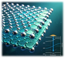
Transition metal dichalcogenides bring something to the table that graphene inherently lacks: a tunable bandgap. In going from bulk to monolayer, MoS2 shifts from an indirect gap of 1.2 eV to a direct gap of 1.8 eV, suddenly making it a strong light emitter and absorber. WS2 adds valley-selective optical response to the mix. WSe2 brings ambipolar transport that enables p-type logic alongside MoS2 n-type channels. MoSe2 pushes electron mobility higher than its sulfide cousins and extends absorption deeper into the infrared. These are not one-size-fits-all materials. They are precision tools, and we grow each one with recipes tailored to its unique chemistry.
- MoS2: n-type dominant, direct gap 1.8 eV (monolayer), strong photoluminescence at 1.9 eV.
- WS2: direct gap, large spin splitting at K valleys, circularly polarized emission under sigma-polarized excitation.
- WSe2: ambipolar field-effect behavior, enabling both electron and hole transport in the same flake.
- MoSe2: higher low-field electron mobility than MoS2, extended infrared photoresponse.
- Growth: CVD on SiO2/Si, sapphire, or mica; mechanical exfoliation flakes also available.
MXenes: Metals in Flatland
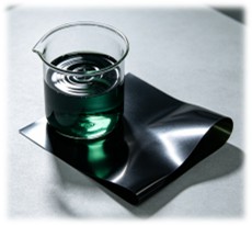
Most 2D materials people talk about are semiconductors or insulators. MXenes break that pattern. These transition metal carbides and nitrides, produced by selectively etching the A-group element from MAX phase ceramics, retain metallic conductivity even down to monolayer thickness. Ti3C2Tx, the most widely studied member, conducts electricity at 8000 S/cm and disperses in water thanks to its hydrophilic surface terminations. That combination of metallic behavior and solution processability opens doors that no other 2D material can walk through.
- Ti3C2Tx: highest conductivity MXene, aqueous colloidal dispersion, film-forming by spray or vacuum filtration.
- Ti2CTx: lighter interlayer structure, favorable for battery electrode intercalation.
- Termination control: -O, -OH, and -F surface groups adjustable via post-etch treatment.
- Form factors: delaminated single-layer dispersion, multilayer clay, or free-standing membrane.
Black Phosphorus: The Anisotropic Outlier
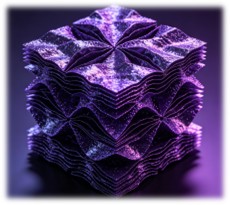
Black phosphorus stands apart. Unlike the isotropic hexagonal lattices of graphene and TMDCs, phosphorene possesses a puckered orthorhombic structure that gives it direction-dependent electrical and thermal conductivity. Its bandgap varies continuously from 0.3 eV in bulk to about 2.0 eV in monolayer form, covering a spectral range that silicon and most TMDCs simply cannot reach. That makes it uniquely valuable for mid-wave infrared detection and anisotropic electronic devices. The catch is air sensitivity, which we address through h-BN encapsulation and controlled-atmosphere packaging.
- Few-layer flakes exfoliated and encapsulated in h-BN for ambient stability.
- Anisotropy ratio up to 2:1 between armchair and zigzag transport directions.
- Bandgap tuneable by thickness, absorbing from 0.6 um to 3.0 um wavelength.
- Hole mobility competitive with silicon at comparable thickness scales.
Graphene Oxide and rGO: Scalable Processability

Not every application demands the pristine perfection of CVD graphene. For bulk composites, membrane separations, and large-area coatings, the processability of graphene oxide often matters more than the pristine electronic structure of as-grown graphene. Our GO is produced by modified Hummers oxidation with tight control over oxidation degree and flake dimensions, while rGO is obtained through reduction protocols that restore conductivity without destroying dispersibility.
- GO: single-layer dominant, 1-20 um lateral size, aqueous dispersion up to 10 mg/mL.
- rGO: C/O ratio >10, electrical conductivity 100-1000 S/m, available as powder or paste.
Where These Materials Make a Difference
The Graphene-Like Series finds its way into an extraordinary range of projects. A few representative arenas where our customers are actively deploying these materials:
- Van der Waals heterostructures: stacking graphene on h-BN on MoS2 creates devices with no lattice-matching constraints, enabling tunnel transistors, excitonic LEDs, and quantum-dot-like confinement.
- Flexible printed electronics: solution-processed MXenes and TMDC inks jet-deposited onto polymer substrates for wearable sensors and conformal antennae.
- Next-generation batteries and supercapacitors: Ti3C2Tx MXene anodes, MoS2 intercalation cathodes, and rGO conductive scaffolds for high-rate energy storage.
- Photonic and optoelectronic systems: MoS2 and WSe2 photodetectors, graphene-h-BN-WS2 tunnel junction emitters, and black phosphorus mid-IR sensors.
- EMI shielding and thermal management: MXene and GNP composites that block electromagnetic interference while dissipating heat in portable electronics.
- Catalysis and environmental remediation: edge-rich MoS2 for hydrogen evolution, MXene membranes for ion-selective filtration, GO adsorbents for pollutant capture.
Characterization That Earns Trust
We characterize every material batch before it ships. Not because regulation demands it, but because reproducible science depends on it. Our in-house metrology suite covers the properties that actually matter for device and process development.
- Raman spectroscopy: layer count verification, defect density quantification via D/G and 2D/G ratios.
- Atomic force microscopy: thickness profiling, surface roughness mapping, and flake dimension measurement.
- Transmission electron microscopy: lattice imaging, grain boundary visualization, and layer stacking confirmation.
- X-ray photoelectron spectroscopy: elemental stoichiometry, oxidation state mapping, and surface termination identification.
- Photoluminescence spectroscopy: direct-gap confirmation for monolayer TMDCs, peak position and linewidth reporting.
- Four-point probe: sheet resistance mapping for conductive films and coatings.
Beyond the Catalog: Custom Synthesis Tailored to Your Workflow
Standard products get you started. Custom materials get you published, patented, and into production. Our synthesis team routinely accommodates requests that fall outside the catalog, from non-standard material compositions to exotic substrate configurations. We have grown h-BN on electroplished Cu with grain sizes exceeding 100 um for single-crystal device studies. We have synthesized MoS2 on 2-inch sapphire wafers for foundry-compatible processing. We have produced MXene compositions beyond the common Ti3C2Tx, including Nb2CTx and Ti2CTx for customers exploring the broader MXene design space. We have encapsulated black phosphorus flakes in h-BN with graphene contacts, delivering ready-to-wire devices.
Whatever your target structure, tell us the material, the substrate, the layer count, and the characterization data you need. We will evaluate the synthesis feasibility, quote a timeline, and deliver a prototype batch for your validation. No minimum order quantity. No pre-set format. Just the material you need, characterized the way you need it.
Start a Conversation
Request a data sheet, ask a technical question, or describe a material configuration that does not exist yet. Our team of materials scientists reads every inquiry and responds with honest feasibility assessments and practical guidance.
| Catalog Number | Product Name | Order | Quantity |
|---|---|---|---|
| GLS-0001 | Few Layers Nano MoS2 Powder (Small Lateral Size) |
-
+
|
|
| GLS-0002 | Small Lateral Size Thin Layer WS2 Dispersion (0.1 mg/mL) |
-
+
|
|
| GLS-0003 | Natural Single Crystal Graphite (99.98%) |
-
+
|
|
| GLS-0004 | WS2 Nanosheet Dispersion (1-10 Layers, 1 mg/mL) |
-
+
|
|
| GLS-0005 | Few Layers WS2 Powder |
-
+
|
|
| GLS-0006 | WS2 Powder (0.88 μm) |
-
+
|
|
| GLS-0007 | Single Layer h-BN Film on Copper Foil (5 cm × 2.5 cm) |
-
+
|
|
| GLS-0008 | Violet Phosphorus Dispersion (0.1 mg/mL) |
-
+
|
|
| GLS-0009 | Monolayer h-BN Film on SiO2/Si Substrate |
-
+
|
|
| GLS-0010 | Multilayer h-BN Film on Nickel Substrate (5-15 Layers) |
-
+
|
For Research or Industrial Raw Materials, Not For Personal Medical Use!