

Products
- High-Quality Graphene
- CVD Graphene, Graphene-Like Materials
- Graphene-Like Series
- Defect-Free Single-Crystal Graphene and Graphene-Like Materials (Mechanical Exfoliation)
- Quantum Dot Series
- Aggregation-Induced Emission (AIE)
- Near-Infrared II (NIR-II) Fluorescent Dyes
- Graphdiyne
- Two-Dimensional Transition Metal Carbides/Nitrides/Borides (MXene)
- Metal Nanomaterials and Other Functional Bio-Nanomaterials
- Metal-Organic Frameworks (MOF)
- Covalent Organic Frameworks (COF)
- Two-Dimensional Layered Metal Oxides (LDH)
- Carbon Nanotube Powders, Pastes
- Carbon Nanotube Arrays and Special Carbon Nanotube Materials
- High-Quality Metallic and Semiconducting High-Purity Single-Walled Carbon Nanotubes
- Carbon Nanotube Sponges
- Mesoporous Carbon and Carbon Nanomaterials
- High-Quality Fullerenes
- One-Dimensional Nanomaterials
- Molecular Sieves
- Inorganic Nanomaterials
- Perovskite Materials
- Highly Oriented Pyrolytic Graphite (HOPG)
- Organic Materials
- Single-Atom Catalysts
- Thermoelectric Materials
- Sodium Storage Materials
- Industrial-Grade Nanomaterials
- Solid-State Lithium Batteries
- Hydrogel Series and Consumables
Online Inquiry
Perovskite Materials
In the span of little more than a decade, metal halide perovskites have risen from obscure laboratory curiosities to the most intensely studied class of solution-processable semiconductors. The archetypal compound methylammonium lead triiodide (MAPbI3) crystallizes in the ABX3 perovskite structure: a three-dimensional network of corner-sharing PbI6 octahedra with methylammonium cations occupying the cuboctahedral cavities. This structure confers a remarkable set of optoelectronic properties: a direct bandgap of approximately 1.5 eV with an exceptionally high absorption coefficient, ambipolar charge transport with electron and hole diffusion lengths exceeding one micrometer in high-quality films, and defect tolerance that enables near-unity internal quantum yields from solution-processed layers. Single-junction solar cells incorporating these materials have achieved certified power conversion efficiencies exceeding 26%, while perovskite-silicon tandem devices have surpassed 31% — approaching the practical limits of photovoltaic energy conversion.
Eata Nanomaterials supplies a comprehensive portfolio of perovskite materials for research and device development. Our catalog includes organic-inorganic hybrid perovskites (MAPbI3, MAPbBr3, FAPbI3, mixed cation/halide compositions), all-inorganic perovskites (CsPbI3, CsPbBr3 quantum dots and polycrystalline films), perovskite single crystals with dimensions up to several centimeters, two-dimensional Ruddlesden-Popper phases for enhanced moisture stability, lead-free alternatives based on tin and germanium, and double perovskites. We further provide high-purity precursor materials including PbI2, MAI, FAI, CsI, and PbBr2 with purity grades suitable for device fabrication, as well as electron and hole transport layer materials such as TiO2, SnO2, Spiro-OMeTAD, and PTAA. Every product is characterized by XRD, UV-Vis spectroscopy, and where applicable, photoluminescence quantum yield measurements.
The Perovskite Crystal Structure and Compositional Tunability
The ABX3 perovskite structure derives its versatility from the geometric flexibility of the corner-sharing BX6 octahedral framework. The Goldschmidt tolerance factor — a dimensionless parameter relating the ionic radii of A, B, and X ions — predicts which compositions will adopt the perovskite structure. For halide perovskites, the A-site can accommodate methylammonium (CH3NH3+), formamidinium (CH(NH2)2+), cesium (Cs+), or rubidium (Rb+); the B-site is typically lead (Pb2+), tin (Sn2+), or germanium (Ge2+); and the X-site is a halide (I-, Br-, Cl- or mixed compositions). This compositional latitude enables continuous bandgap tuning from 1.2 eV (FASnI3) to 3.0 eV (CsPbCl3), spanning the entire visible spectrum and parts of the infrared and ultraviolet.
Mixed-cation and mixed-halide strategies further expand the engineering toolbox. Partial substitution of formamidinium with cesium and methylammonium stabilizes the photoactive black phase of FAPbI3, suppressing the formation of the undesirable yellow non-perovskite polymorph. Bromide incorporation into iodide perovskites raises the bandgap for tandem cell applications, while chloride addition (typically below 5%) improves carrier mobility and reduces recombination. The ability to fine-tune optical and electronic properties through simple solution mixing — without changing the underlying crystal structure — makes perovskites uniquely adaptable to diverse device architectures.
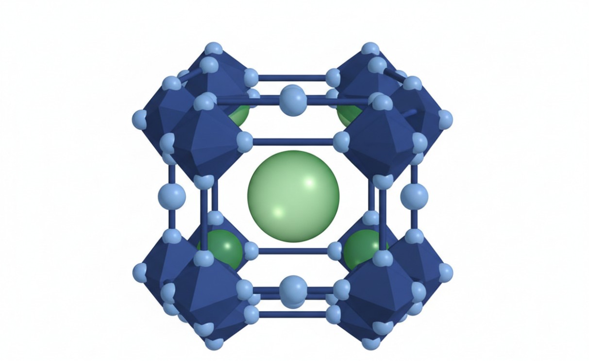 Crystal structure of an ABX3 perovskite showing corner-sharing BX6 octahedra and A-site cations in the cuboctahedral cavities
Perovskite Solar Cells: From Single-Junction to Tandem Architectures
Perovskite solar cells have demonstrated a trajectory of efficiency improvement unprecedented in photovoltaic history. The standard n-i-p device architecture stacks a transparent conductive oxide (FTO or ITO), an electron transport layer (TiO2 or SnO2), the perovskite absorber (typically 400–800 nm thick), a hole transport layer (Spiro-OMeTAD, PTAA, or PEDOT:PSS), and a metal back contact (Au or Ag). Inverted p-i-n architectures place the hole transport layer beneath the perovskite, enabling lower-temperature processing and improved compatibility with tandem configurations. Certified efficiencies now exceed 26% for single-junction cells, with recent advances in bilayer electron transport engineering — combining C70 for rapid electron extraction and C60 for efficient charge transport — delivering PCE values of 24.51% with excellent reproducibility.
Tandem devices that stack a wide-bandgap perovskite top cell atop a silicon bottom cell have shattered the single-junction efficiency ceiling, achieving certified efficiencies of 31.46% at 1 cm2 aperture area. All-perovskite tandems combining a wide-bandgap lead-mixed-halide front cell with a narrow-bandgap tin-lead rear cell have surpassed 29% efficiency, while perovskite-organic hybrids have reached 25.06%. The key to these remarkable figures lies in meticulous interface engineering: self-assembled monolayers for hole extraction, CuSCN for grain boundary passivation, and optimized transport layer band alignment that minimizes interfacial recombination while maximizing photocurrent.
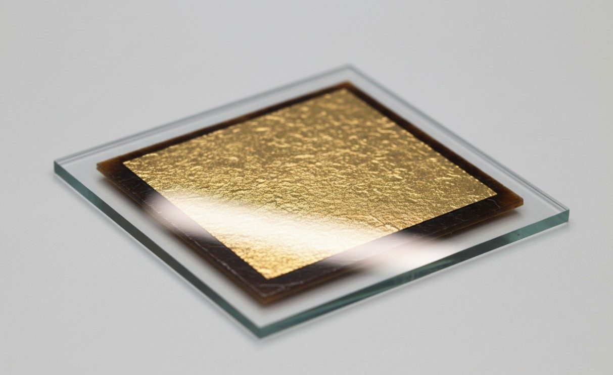 Thin-film perovskite solar cell device on a transparent glass substrate with gold top electrode
All-Inorganic Perovskites and Quantum Dots
While hybrid organic-inorganic perovskites dominate the photovoltaic landscape, their organic components introduce thermal and moisture sensitivity that limits operational stability. All-inorganic perovskites — exemplified by cesium lead halides (CsPbX3, X = Cl, Br, I) — replace the volatile organic cation with cesium, yielding materials that retain the exceptional optoelectronic properties of their hybrid cousins while withstanding temperatures exceeding 200 C. At the nanoscale, CsPbX3 quantum dots exhibit size-tunable emission spanning the entire visible spectrum (420–700 nm) with photoluminescence quantum yields exceeding 90%, narrow emission linewidths (full width at half maximum of 12–40 nm), and high defect tolerance that enables facile room-temperature synthesis.
These properties have propelled perovskite quantum dots to the forefront of display technology research. Their narrow emission bandwidths satisfy the Rec. 2020 color gamut requirements for next-generation ultrahigh-definition displays, while solution processability enables printing and coating techniques incompatible with conventional CdSe quantum dots. In lighting, perovskite quantum dots serve as down-conversion layers for white LEDs with color rendering indices exceeding 90. We supply CsPbX3 quantum dots as colloidal dispersions in toluene or hexane, with emission peaks precisely tuned by halide composition and quantum confinement. Custom surface ligand exchange — replacing oleic acid/oleylamine with shorter-chain ligands for enhanced charge transport — is available upon request.
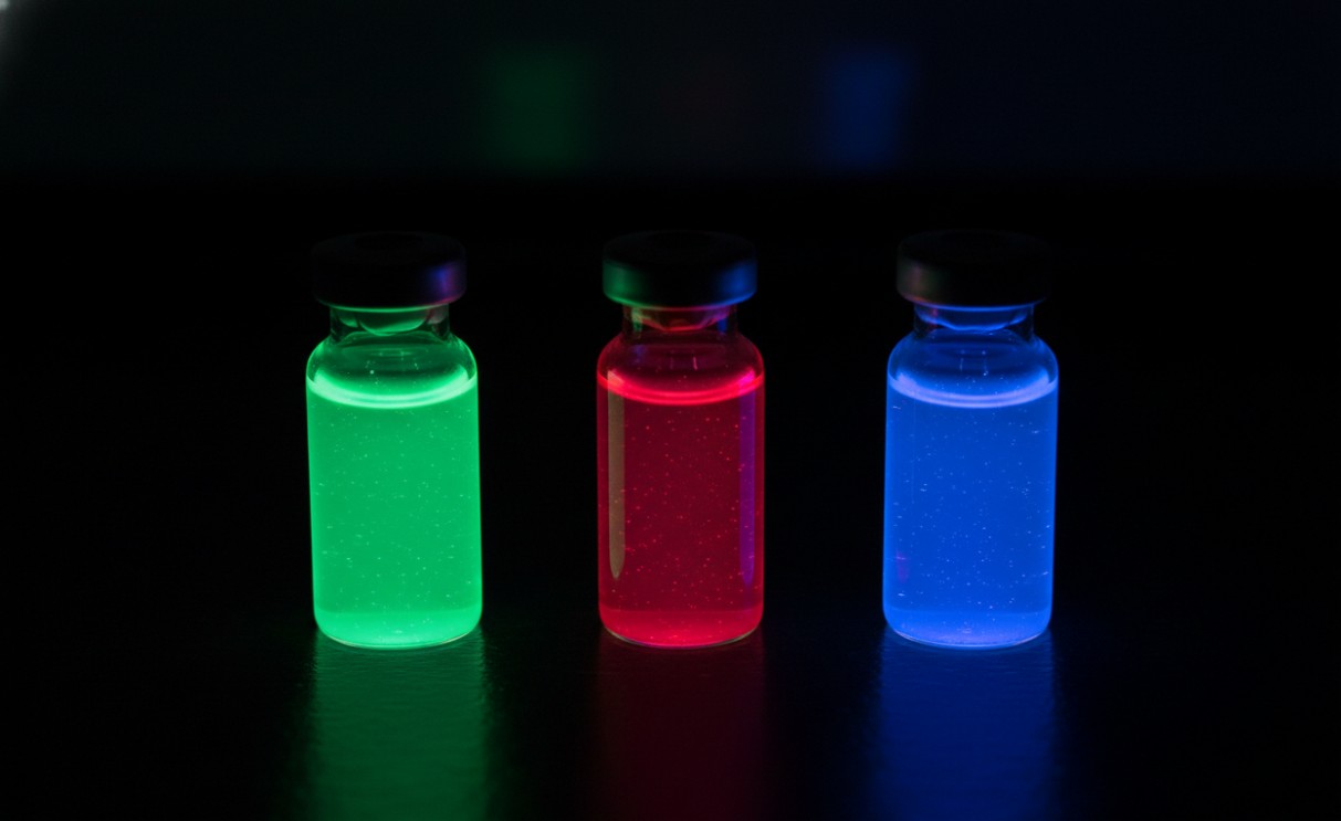 All-inorganic cesium lead halide perovskite quantum dots exhibiting vivid green, red, and blue photoluminescence under UV excitation
Perovskite Single Crystals
Polycrystalline perovskite films suffer from grain boundary defects that trap charge carriers and accelerate degradation under illumination and humidity. Single crystals eliminate these boundaries entirely, offering diffusion lengths exceeding 175 micrometers — over 100 times those of polycrystalline films — and trap state densities below 10^10 cm^-3. These extraordinary transport properties make perovskite single crystals ideal substrates for fundamental studies of carrier dynamics, as well as active layers for high-sensitivity X-ray detectors, gamma-ray spectrometers, and photodetectors with specific detectivities rivaling commercial silicon and InGaAs devices.
We grow perovskite single crystals by several methods: inverse temperature crystallization (ITC) for rapid growth of millimeter-scale MAPbI3 crystals in solution; antisolvent vapor-assisted crystallization (AVC) for high-quality crystals with low defect density; and Bridgman growth for centimeter-scale boules. Available compositions include MAPbI3, MAPbBr3, FAPbI3, and mixed cation crystals tailored for specific bandgap requirements. Crystals are supplied as as-grown boules, polished wafers, or diced chips, with surface roughness below 1 nm achievable for epitaxy-grade substrates. Custom doping with bismuth, europium, or manganese enables the exploration of new physical phenomena including ferroelectricity, multiferroicity, and single-photon emission.
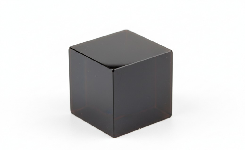 High-quality cubic perovskite single crystal with mirror-like reflective facets and sharp edges
Two-Dimensional and Lead-Free Perovskites
Two-dimensional Ruddlesden-Popper perovskites insert large organic spacer cations — typically long-chain alkylammoniums or aromatic amines — between inorganic perovskite layers, creating a natural quantum well structure where the inorganic layers function as semiconductor wells and the organic spacers as insulating barriers. These materials exhibit enhanced moisture resistance due to the hydrophobic nature of the organic spacers, high exciton binding energies that enable pure excitonic emission for narrow-linewidth LEDs, and structural diversity that permits the tuning of layer thickness from monolayer (n=1) to near-bulk (n > 5). Our catalog includes phenylethylammonium (PEA), butylammonium (BA), and octylammonium (OA) based 2D perovskites with lead, tin, and germanium B-site cations.
Environmental and health concerns surrounding lead have catalyzed intensive research into lead-free alternatives. Tin-based perovskites (FASnI3, MASnI3) offer bandgaps of 1.2–1.4 eV and demonstrate PCE values exceeding 14% in solar cells, though their susceptibility to Sn2+ oxidation to Sn4+ remains a significant challenge requiring glovebox processing and antioxidant additives. Germanium-based perovskites explore the frontiers of lead-free materials, with recent studies demonstrating polar structures and second harmonic generation in two-dimensional germanium iodide perovskites. Double perovskites such as Cs2AgBiBr6 — where two B-site cations (Ag+ and Bi3+) replace the single Pb2+ — provide a different route to lead-free optoelectronics with enhanced stability but lower absorption coefficients. We supply these emerging materials for researchers pioneering the next generation of sustainable perovskite technology.
Featured Products
| Products | Specifications | Applications |
| MAPbI3 powder/film | Bandgap: 1.5 eV; Cubic; Purity >99.9% | Single-junction solar cells |
| FAPbI3 powder/film | Bandgap: 1.48 eV; Black phase; High purity | High-efficiency PSCs, tandems |
| CsPbX3 quantum dots | PLQY: >90%; FWHM: 12-40 nm; Emission tunable | Displays, LEDs, bioimaging |
| Perovskite single crystal | Diffusion length: >175 um; Trap density: <10^10 cm^-3 | X-ray detectors, photodetectors |
| 2D RP perovskite | PEA/BA/OA spacer; n=1-5; Moisture stable | Narrow-linewidth LEDs |
| Sn-based lead-free | FASnI3, MASnI3; Bandgap: 1.2-1.4 eV | Lead-free solar cells |
| Double perovskite | Cs2AgBiBr6; Lead-free; Stable | Stable optoelectronics |
| Precursor materials | PbI2, MAI, FAI, CsI, PbBr2; >99.99% | Device fabrication |
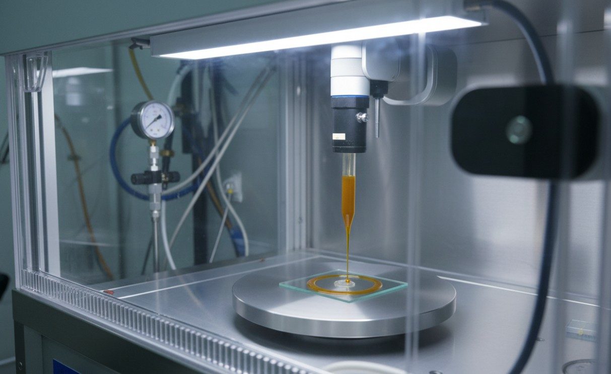 Spin-coating setup depositing perovskite precursor solution onto a substrate in a nitrogen-filled glovebox environment
Applications Across Research and Industry
Single-Junction Solar Cells: Certified efficiencies exceeding 26% in n-i-p and p-i-n architectures, with optimized transport layers enabling fill factors above 80%.
Tandem Photovoltaics: Perovskite-silicon tandems surpass 31% efficiency; all-perovskite tandems exceed 29%; perovskite-organic hybrids reach 25%.
Perovskite LEDs: External quantum efficiencies exceeding 28% for green emitters, with narrow linewidths enabling wide-color-gamut displays.
Quantum Dot Displays: CsPbX3 quantum dots with PLQY >90% and FWHM of 12–40 nm satisfy Rec. 2020 color gamut for next-generation displays.
X-Ray and Gamma Detection: Perovskite single crystals with diffusion lengths >175 um and low trap densities enable high-sensitivity radiation detection.
Photodetectors: Broadband response from ultraviolet to near-infrared with specific detectivities rivaling commercial Si and InGaAs devices.
Quality Assurance and Characterization
Every perovskite product undergoes rigorous analytical characterization before shipment. Powder X-ray diffraction (XRD) confirms phase purity and identifies any non-perovskite polymorphs or decomposition products. UV-Vis absorption spectroscopy verifies bandgap energy and optical quality. Photoluminescence spectroscopy measures emission peak position, linewidth, and — for quantum dots and single crystals — photoluminescence quantum yield. Thermogravimetric analysis evaluates thermal stability and decomposition temperature. For device-grade materials, we additionally assess film morphology by scanning electron microscopy (SEM), carrier dynamics by time-resolved photoluminescence (TRPL), and composition by energy-dispersive X-ray spectroscopy (EDS) or X-ray photoelectron spectroscopy (XPS). Precursor materials are characterized by inductively coupled plasma optical emission spectroscopy (ICP-OES) to verify metal content and by proton NMR to confirm organic purity. All data are provided in a comprehensive certificate of analysis.
Custom Synthesis and Formulation Services
We welcome collaborative projects that push the boundaries of perovskite materials development. Our capabilities include custom composition tuning — mixed A-site, B-site, and X-site formulations with precise stoichiometric control; surface functionalization with custom ligands for quantum dots and nanocrystals; film deposition services including spin-coating, blade-coating, and vacuum thermal evaporation on customer-supplied or in-house substrates; doping studies with transition metals, lanthanides, or main group elements for targeted property modification; and scale-up from milligram laboratory samples to gram and multi-gram batches for device fabrication campaigns. Whether you require a novel composition for a fundamental study, a device-grade film for a fabrication run, or a tailored quantum dot ink for a display prototype, our team is prepared to design and deliver materials that meet your exact specifications.
Request a Quote— Contact Eata Nanomaterials to discuss your perovskite material requirements, request product samples, or explore a custom synthesis and formulation engagement for your solar cell, LED, or optoelectronic research program.
| Catalog Number | Product Name | Order | Quantity |
|---|---|---|---|
| PERM-0001 | Methylammonium Lead Iodide (MAPbI3) Perovskite Spin Coating Solution |
-
+
|
|
| PERM-0002 | Methylammonium Iodide (MAI) |
-
+
|
|
| PERM-0003 | Cs2ZrxSnyCl6:Te Perovskite Microcrystal |
-
+
|
|
| PERM-0004 | CsPbCl1.5Br1.5 Perovskite Quantum Dot Dispersion |
-
+
|
|
| PERM-0005 | CsPbClBr2 Perovskite Quantum Dot Dispersion |
-
+
|
|
| PERM-0006 | CsPbBr2I Perovskite Quantum Dot Dispersion |
-
+
|
|
| PERM-0007 | CsPbI2Br Perovskite Quantum Dot Dispersion |
-
+
|
|
| PERM-0008 | CsPbBr3 Perovskite Quantum Dot Dispersion |
-
+
|
|
| PERM-0009 | CsPbCl3 Perovskite Quantum Dot Dispersion |
-
+
|
|
| PERM-0010 | CsPbI3 Perovskite Quantum Dot Dispersion |
-
+
|
For Research or Industrial Raw Materials, Not For Personal Medical Use!