

Products
- High-Quality Graphene
- CVD Graphene, Graphene-Like Materials
- Graphene-Like Series
- Defect-Free Single-Crystal Graphene and Graphene-Like Materials (Mechanical Exfoliation)
- Quantum Dot Series
- Aggregation-Induced Emission (AIE)
- Near-Infrared II (NIR-II) Fluorescent Dyes
- Graphdiyne
- Two-Dimensional Transition Metal Carbides/Nitrides/Borides (MXene)
- Metal Nanomaterials and Other Functional Bio-Nanomaterials
- Metal-Organic Frameworks (MOF)
- Covalent Organic Frameworks (COF)
- Two-Dimensional Layered Metal Oxides (LDH)
- Carbon Nanotube Powders, Pastes
- Carbon Nanotube Arrays and Special Carbon Nanotube Materials
- High-Quality Metallic and Semiconducting High-Purity Single-Walled Carbon Nanotubes
- Carbon Nanotube Sponges
- Mesoporous Carbon and Carbon Nanomaterials
- High-Quality Fullerenes
- One-Dimensional Nanomaterials
- Molecular Sieves
- Inorganic Nanomaterials
- Perovskite Materials
- Highly Oriented Pyrolytic Graphite (HOPG)
- Organic Materials
- Single-Atom Catalysts
- Thermoelectric Materials
- Sodium Storage Materials
- Industrial-Grade Nanomaterials
- Solid-State Lithium Batteries
- Hydrogel Series and Consumables
Online Inquiry
One-Dimensional Nanomaterials
When matter is sculpted into one-dimensional form — long filaments with diameters measured in nanometers — something extraordinary happens. Electrons, photons, and phonons that move freely in bulk crystals become confined along two spatial dimensions, amplifying quantum effects and giving rise to properties unattainable in their parent materials. A silicon nanowire with a diameter below 10 nm exhibits a direct bandgap despite silicon being an indirect semiconductor in bulk form. A zinc oxide nanowire grown vertically on a substrate functions as a minuscule laser cavity, generating ultraviolet light at room temperature. A silver nanowire mesh on a plastic sheet conducts electricity while remaining virtually invisible to the eye. These are not laboratory curiosities; they are the functional elements of tomorrow's electronics, energy systems, and sensing platforms.
Eata Nanomaterials produces an extensive portfolio of one-dimensional nanomaterials spanning metallic, semiconducting, and ceramic compositions. Our collection includes silver nanowires for transparent conductors, silicon nanowires for high-mobility transistors, zinc oxide and gallium nitride nanowires for optoelectronics and sensing, titanium dioxide nanotube arrays for photocatalysis and energy storage, iron oxide nanorods for catalysis and magnetic separation, and core-shell heterostructure nanowires that marry disparate functionalities within a single filament. Each material is available as a colloidal dispersion, a substrate-grown aligned array, or a dry powder — with full characterization data provided for every batch.
Semiconductor Nanowires: ZnO, GaN, and Silicon
Semiconductor nanowires occupy a special place in the nanomaterials toolkit because their diameter-dependent bandgap, enhanced surface-to-volume ratio, and efficient axial carrier transport make them uniquely suited for optoelectronic and electronic device applications. Our ZnO nanowires, grown by vapor-liquid-solid (VLS) or chemical vapor deposition (CVD) on sapphire, silicon, or flexible polymer substrates, exhibit diameters from 20 to 200 nm and lengths up to tens of micrometers. Their wide direct bandgap of 3.37 eV, combined with a large exciton binding energy of 60 meV, supports room-temperature ultraviolet lasing and high-sensitivity gas detection.
Gallium nitride nanowires push the optoelectronic envelope further into the deep ultraviolet. With a bandgap of 3.42 eV and robust thermal stability, GaN nanowires serve as building blocks for UV LEDs, laser diodes, and high-power transistors capable of operating at temperatures and frequencies that would destroy conventional silicon devices. Silicon nanowires, meanwhile, offer a pathway to extend Moore's Law beyond the planar limit. Their diameter-tunable bandgap enables tunnel field-effect transistors with sub-60 mV/decade subthreshold swing — a feat impossible in bulk silicon — while their enhanced surface area boosts lithium-ion battery capacity when used as anode material.
 Scanning electron micrograph of vertically aligned zinc oxide nanowires grown on a substrate showing hexagonal cross-sections
Metal Nanowires: Silver, Gold, and Copper
Metal nanowires leverage the exceptional electrical conductivity of their parent metals while adding mechanical flexibility and optical transparency through their filamentary geometry. Silver nanowires have emerged as the leading replacement for indium tin oxide (ITO) in flexible transparent conductors: a random network of silver nanowires with diameters of 20–100 nm and lengths of 5–50 micrometers achieves sheet resistances below 50 ohm per square at optical transmittances exceeding 90%, all while surviving thousands of bending cycles around a 5 mm radius.
Our silver nanowires are synthesized by the polyol method — reducing silver nitrate in ethylene glycol with polyvinylpyrrolidone (PVP) as a capping agent — yielding high-aspect-ratio nanowires with aspect ratios exceeding 200. Copper nanowires offer a lower-cost alternative with comparable conductivity, synthesized through aqueous reduction routes. Gold nanowires, produced by oleylamine-mediated growth or template electrodeposition, find application in plasmonic devices, biosensors, and stretchable electronics where chemical stability is paramount. We supply metal nanowires as aqueous or ethanolic dispersions, as spray-coated films on PET or glass substrates, and as dry powders.
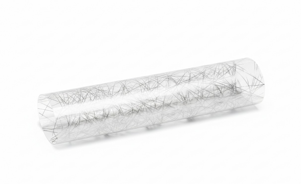 Flexible transparent electrode film composed of a silver nanowire network embedded in a polymer substrate
TiO2 Nanotube Arrays by Electrochemical Anodization
Titanium dioxide nanotube arrays represent a unique class of one-dimensional nanomaterials produced not by vapor-phase growth but by electrochemical anodization of titanium metal in fluoride-containing electrolytes. Under carefully controlled voltage, a self-organized hexagonal array of vertically oriented nanotubes emerges on the titanium surface, with tube diameters tunable from 20 to 200 nm by adjusting the applied potential, and lengths extendable to hundreds of micrometers by controlling anodization time and electrolyte composition.
These highly ordered arrays possess several compelling attributes: an extremely high surface area-to-volume ratio, unidirectional electron transport along the tube axis, and the ability to absorb light efficiently due to photon trapping within the tubular architecture. After annealing at 400–500 C, the as-formed amorphous nanotubes crystallize into the anatase phase, activating photocatalytic properties that enable water splitting, dye degradation, and antibacterial action under UV illumination. Doping with nitrogen or coupling with narrow-bandgap semiconductors extends photocatalytic activity into the visible range. In energy storage, TiO2 nanotube arrays serve as high-rate anodes for lithium-ion batteries and as photoanodes for dye-sensitized solar cells, where the vertically oriented architecture accelerates charge collection and reduces recombination losses.
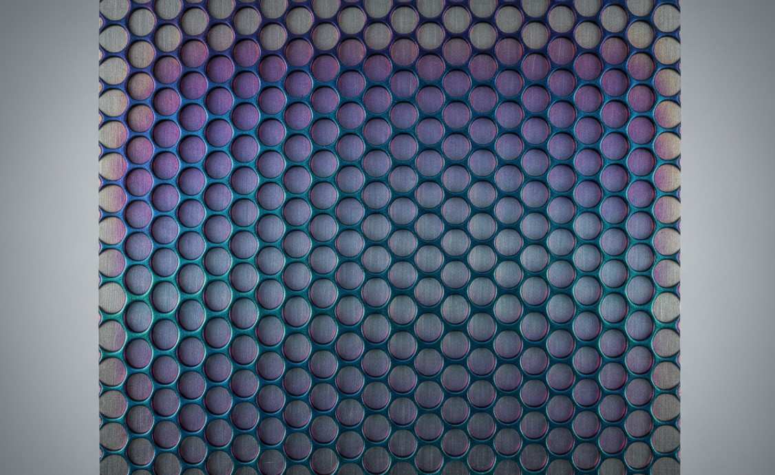 Top-down view of a highly ordered titanium dioxide nanotube array showing hexagonal honeycomb pore structure with iridescent coloration
Core-Shell and Heterostructure Nanowires
The functionality of a nanowire can be dramatically expanded by coating it with a shell of a different material, creating a core-shell heterostructure that combines the best properties of both constituents. A silicon nanowire core wrapped in a silicon dioxide shell gains passivation against oxidation while maintaining high carrier mobility — a configuration that has enabled record-breaking nanowire transistor performance. A zinc oxide nanowire sheathed in titanium dioxide functions as a photocatalytic antenna: ZnO absorbs UV light and generates electron-hole pairs, while the TiO2 shell provides catalytic sites for redox reactions and suppresses photocorrosion of the underlying ZnO.
We fabricate core-shell nanowires through sequential CVD or atomic layer deposition (ALD) processes that deposit conformal coatings as thin as a few nanometers with sub-nanometer precision. Available core-shell combinations include Si/SiO2, ZnO/TiO2, Ag/SiO2, Cu/Ni, and GaN/AlGaN, with custom heterostructures developed upon request. These architectures find application in passivated nanowire electronics, photocatalytic water treatment, plasmon-enhanced sensing, and magnetic nanocomposites where the shell prevents aggregation and oxidation of the metallic core.
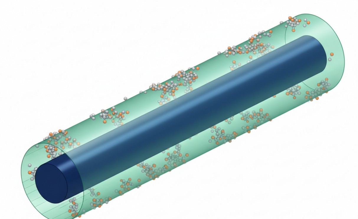 Cross-sectional illustration of a core-shell nanowire heterostructure with a central core surrounded by a concentric shell layer
Applications Across Research and Industry
Flexible Transparent Electronics: Silver nanowire networks replace ITO in foldable displays, touch screens, and wearable sensors, offering comparable conductivity with superior mechanical resilience.
UV Optoelectronics: ZnO and GaN nanowires emit and detect ultraviolet light for sterilization systems, flame sensors, and high-density optical data storage.
Photocatalysis and Water Treatment: TiO2 nanotube arrays and ZnO/TiO2 core-shell nanowires degrade organic pollutants and split water for hydrogen production under solar illumination.
High-Performance Batteries: Silicon nanowire anodes accommodate volume expansion during lithiation, delivering capacities several times higher than graphite while maintaining cycle stability.
Chemical and Biosensing: The large surface area and size-dependent optical properties of metal and semiconductor nanowires enable label-free detection of biomolecules, gases, and environmental contaminants at ppb concentrations.
Catalysis: Iron oxide nanorods and noble metal nanowires serve as active catalysts and supports for reactions ranging from CO oxidation to electrochemical water splitting.
Featured Products
| Products | Specifications | Applications |
| Silver nanowires | D: 20–100 nm; L: 5–50 um; Aspect ratio >200 | Transparent conductors, sensors |
| Silicon nanowires | D: 10–200 nm; Single-crystal; VLS grown | Transistors, battery anodes |
| ZnO nanowires | D: 20–200 nm; Bandgap: 3.37 eV; Wurtzite | UV lasers, gas sensors |
| GaN nanowires | D: 50–300 nm; Bandgap: 3.42 eV | UV LEDs, power electronics |
| TiO2 nanotube arrays | D: 20–200 nm; Length: up to hundreds of um | Photocatalysis, batteries |
| Fe2O3 nanorods | D: 20–100 nm; Magnetic; Hematite | Catalysis, separation |
| Core-shell nanowires | Si/SiO2, ZnO/TiO2, Ag/SiO2 | Passivated electronics |
| Copper nanowires | D: 50–200 nm; Low-cost alternative to Ag | Transparent electrodes |
 Glass vials containing colloidal dispersions of various one-dimensional nanomaterials showing characteristic colors
Quality Assurance and Characterization
Every batch of one-dimensional nanomaterials undergoes rigorous quality control before release. Scanning electron microscopy (SEM) documents morphology, dimensions, and aspect ratio. Transmission electron microscopy (TEM) resolves crystallinity, growth direction, and core-shell interface quality. X-ray diffraction (XRD) confirms phase purity and crystallographic orientation. For semiconductor nanowires, photoluminescence spectroscopy verifies optical quality and bandgap energy. For metal nanowires, four-point probe measurements report electrical conductivity of networked films. Dynamic light scattering (DLS) and zeta potential measurements characterize dispersion stability. Thermogravimetric analysis quantifies residual surfactant or capping agent content. All data are compiled into a certificate of analysis that ships with every order.
Tailored Growth and Custom Architectures
We welcome collaborative projects that push beyond our standard offerings. Our engineering team can grow nanowire arrays on custom substrates — including patterned wafers, flexible polymers, and metal foils — with controlled diameter, length, and areal density. We can synthesize alloy nanowires (such as ZnMgO or InGaN) for bandgap engineering, fabricate axial or radial heterojunctions for device integration, and apply surface functionalization with carboxyl, amine, or thiol groups for biological conjugation. For applications requiring specific morphologies, we can produce branched nanowires, nanotetrapods, and nanobelts. Whatever your one-dimensional nanomaterial requirements, we are prepared to design a synthesis protocol that meets your specifications.
Contact Us— Reach out to Eata Nanomaterials to discuss your one-dimensional nanomaterial requirements, request samples for evaluation, or explore a custom synthesis project tailored to your research or industrial application.
| Catalog Number | Product Name | Order | Quantity |
|---|---|---|---|
| ODN-0001 | Silver Nanowires 40-60 nm |
-
+
|
|
| ODN-0002 | Hydroxypropyl Cellulose Photonic Crystal |
-
+
|
|
| ODN-0003 | TEMPO Oxidized Cellulose Nanofibers |
-
+
|
|
| ODN-0004 | Zinc Oxide Nanowires |
-
+
|
|
| ODN-0005 | Carboxylated Cellulose Nanocrystals |
-
+
|
|
| ODN-0006 | Sulfonated Cellulose Nanocrystals |
-
+
|
|
| ODN-0007 | Pure Hydroxyl-Containing Cellulose Nanocrystals |
-
+
|
|
| ODN-0008 | Bifunctional Cellulose Nanocrystals |
-
+
|
|
| ODN-0009 | Lignocellulose Nanocrystals |
-
+
|
|
| ODN-0010 | Dialdehyde Cellulose Nanocrystals |
-
+
|
For Research or Industrial Raw Materials, Not For Personal Medical Use!