

Nanomaterial-Enhanced Coating and Film Development Services
The performance of a coating is ultimately determined by phenomena occurring at the nanometer scale. A corrosion-resistant layer only a few hundred nanometers thick can extend the service life of a steel component by decades. A superhydrophobic surface with micro-nano hierarchical roughness repels water more effectively than any bulk material. An optical thin film stack precisely engineered at the atomic level controls the transmission and reflection of light across specific wavelength bands. These capabilities emerge when nanomaterials science meets thin-film deposition technology.
Eata Nanomaterials operates a coating development laboratory equipped with multiple deposition platforms spanning gas-phase, solution-phase, and spray-based methods. We design and fabricate nanostructured coatings on metals, ceramics, semiconductors, and polymers, tailoring thickness, composition, morphology, and crystallinity to meet application-specific functional requirements. Whether the need is a single-layer anti-corrosion barrier or a multi-functional coating combining hydrophobicity, UV protection, and scratch resistance, our development pipeline delivers validated coating solutions.
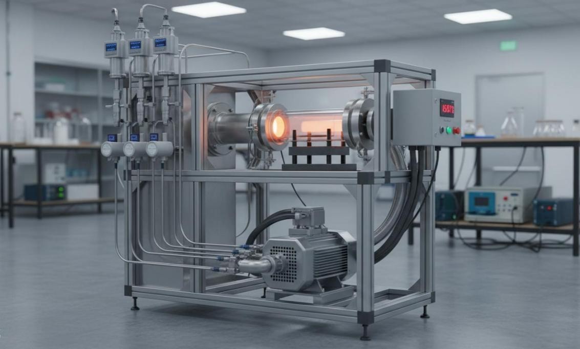 Figure 1: A horizontal tube furnace CVD system with precursor gas delivery lines, heated reaction zone, and substrate holder for depositing conformal nanostructured thin films.
Vapor-Phase Deposition: CVD, PVD, and ALD
Vapor-phase deposition methods offer unmatched control over film composition, thickness, and microstructure. At Eata Nanomaterials, we operate three complementary vapor-phase platforms, each selected based on the substrate geometry, material system, and performance targets:
- Chemical vapor deposition produces high-quality dense films through chemical reactions of precursor gases on a heated substrate surface. Our LPCVD and PECVD systems deposit silicon dioxide, silicon nitride, titanium dioxide, and amorphous carbon films at temperatures from 200 to 800 degrees Celsius. PECVD extends the capability to temperature-sensitive polymer substrates by using plasma activation to reduce deposition temperature below 150 degrees Celsius while maintaining film density and adhesion
- Physical vapor deposition via DC and RF magnetron sputtering deposits metallic, ceramic, and compound semiconductor films with excellent thickness uniformity and adhesion. Our multi-target sputtering system enables reactive sputtering of oxides and nitrides, co-sputtering of alloy compositions, and multilayer deposition without breaking vacuum. Typical film thicknesses range from 10 nanometers to several micrometers with uniformity better than 5 percent across 100-millimeter substrates
- Atomic layer deposition achieves angstrom-level thickness precision through self-limiting surface reactions. By introducing precursors sequentially with purge steps between each exposure, ALD deposits one atomic layer per cycle, enabling conformal coating over complex 3D geometries, high-aspect-ratio trenches, and porous structures inaccessible to line-of-sight methods. Our thermal ALD system deposits Al2O3, TiO2, ZnO, HfO2, and Ru thin films at temperatures as low as 90 degrees Celsius, making ALD compatible with polymer templates and biological substrates
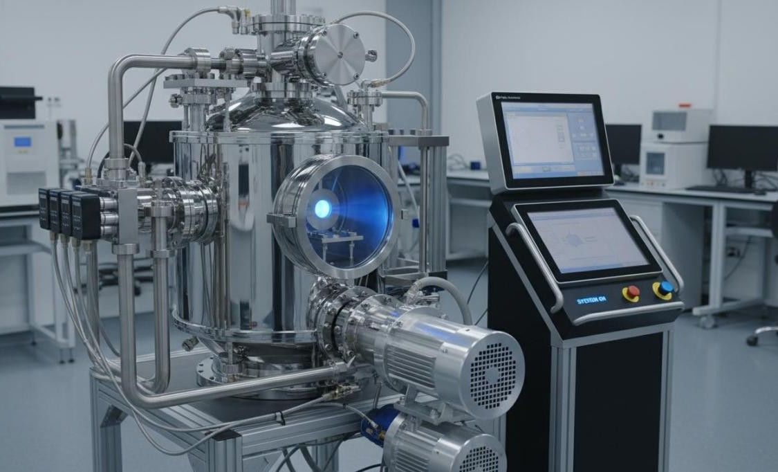 Figure 2: A PVD magnetron sputtering system with a cylindrical stainless steel vacuum chamber, blue plasma glow, circular target, and substrate holder connected to turbomolecular pump and process gas supply.
Solution-Based Coating Methods
For applications requiring thicker films, large-area coating, or lower equipment costs, solution-based methods provide practical and scalable alternatives to vapor-phase deposition. Our wet-chemistry coating capabilities include:
- Sol-gel processing for depositing metal oxide and hybrid organic-inorganic coatings through hydrolysis and condensation of metal alkoxide precursors. The sol-gel method enables composition tuning through precursor blending, porosity control through drying conditions, and crystallinity control through thermal annealing. We formulate sol-gel coatings of SiO2, TiO2, Al2O3, and ZrO2 with thicknesses from 50 nanometers to several micrometers on substrates ranging from silicon wafers to architectural glass panels
- Dip coating for applying uniform thin films on substrates with complex shapes. By controlling withdrawal speed and sol viscosity, film thickness follows the Landau-Levich relationship, enabling predictable thickness from 20 to 500 nanometers. This method is particularly suited for coating optical lenses, fibers, and 3D-printed components
- Spin coating for rapid, uniform film formation on flat substrates. By adjusting spin speed and sol properties, we achieve thickness control from 10 nanometers to 10 micrometers with uniformity better than 2 percent across standard wafer sizes. Spin coating is our primary method for preparing perovskite quantum dot films and photoresist-like nanocomposite layers
- Spray coating for large-area and flexible substrates that cannot be accommodated in vacuum chambers or spin coaters. Our automated spray system with programmable spray gun motion delivers uniform coatings on substrates up to 300 by 300 millimeters, with adjustable spray parameters for coating porosity and surface roughness
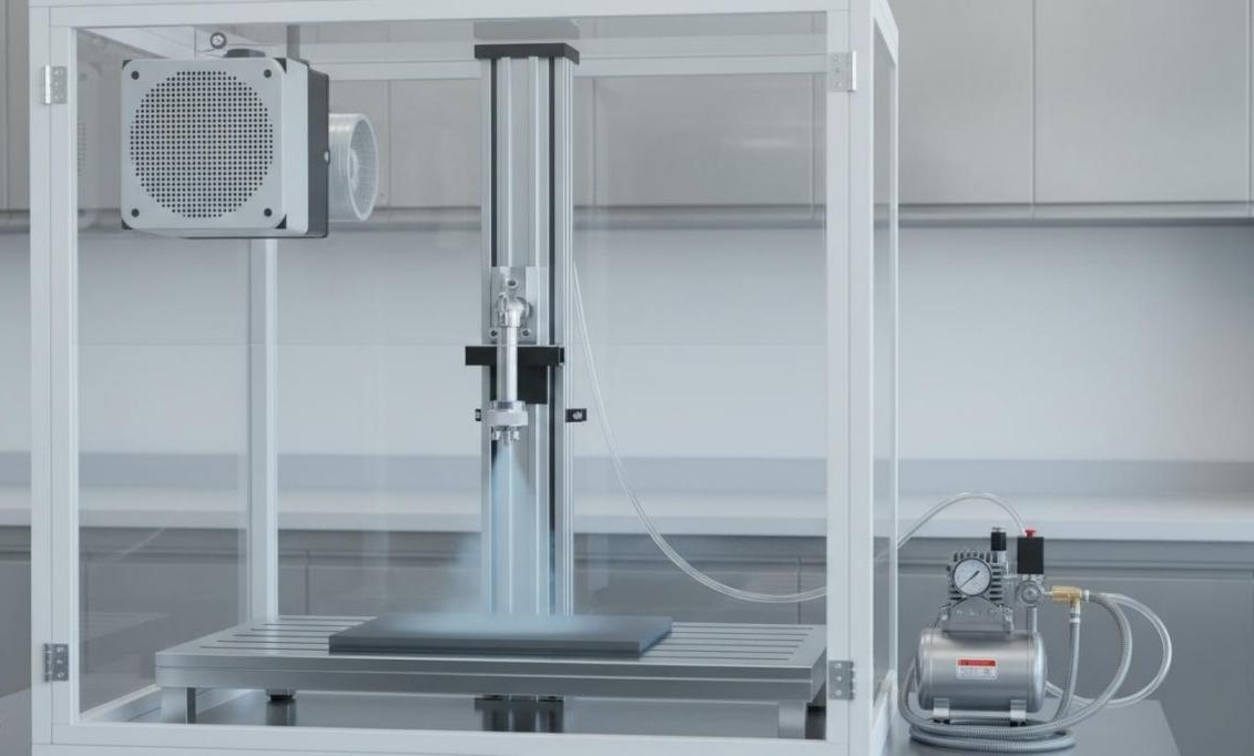 Figure 3: An automated spray coating system with a spray gun on a vertical linear motion stage above a substrate table, enclosed in a ventilated chamber with HEPA filtration.
Superhydrophobic and Self-Cleaning Nanocoatings
Inspired by the lotus leaf, superhydrophobic surfaces exhibit water contact angles exceeding 150 degrees and sliding angles below 10 degrees, enabling water droplets to roll off while collecting and removing surface contaminants. The key to artificial superhydrophobicity lies in creating a dual-scale micro-nano surface roughness combined with a low-surface-energy chemical modification.
Eata Nanomaterials develops superhydrophobic coatings through two complementary approaches:
- Top-down methods including laser ablation, plasma etching, and chemical etching to create hierarchical roughness on metal, silicon, and glass substrates, followed by fluorosilane or fluoropolymer grafting to reduce surface energy. These methods produce durable superhydrophobic surfaces with contact angles above 160 degrees and excellent mechanical robustness
- Bottom-up methods depositing nanoparticle-based coatings that self-organize into hierarchical structures during solvent evaporation. Silica or titania nanoparticles are dispersed in a binder system, applied by spray or dip coating, and cured to create a stable nanostructured surface. This approach is cost-effective for large-area applications and can be applied to substrates of virtually any geometry
Superhydrophobic coatings from Eata Nanomaterials are validated through contact angle goniometry, sliding angle measurement, and long-term durability testing including UV exposure, thermal cycling, and mechanical abrasion. Applications include anti-icing coatings for aerospace, self-cleaning architectural surfaces, anti-corrosion protection for marine components, and anti-fouling treatments for medical devices.
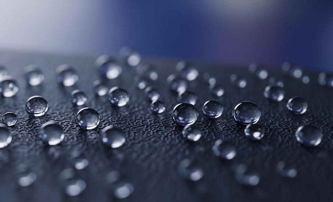 Figure 4: A superhydrophobic nanocoated surface showing perfectly spherical water droplets with contact angles exceeding 150 degrees, demonstrating extreme water repellency.
Anti-Corrosion and Protective Nanocoatings
Corrosion causes economic losses exceeding 3 percent of global GDP annually. Nanostructured coatings offer a compelling defense strategy by combining barrier properties with active corrosion inhibition at dramatically reduced thickness compared to conventional paint systems.
Our anti-corrosion coating development capabilities span:
- Ceramic barrier coatings of Al2O3, SiO2, and Si3N4 deposited by ALD or CVD to hermetically seal metal surfaces from moisture and oxygen. At 50 to 200 nanometers thickness, these coatings provide barrier performance equivalent to micrometer-thick polymer coatings, without the pinhole defects that plague thicker organic layers
- Sol-gel based hybrid coatings incorporating silica nanoparticles in an organosilane matrix, combining the barrier properties of SiO2 with the flexibility and adhesion of organic components. These coatings cure at room temperature, making them suitable for field application on existing infrastructure
- Graphene oxide and reduced graphene oxide coatings that exploit the impermeability of graphene sheets to gas and liquid molecules. GO coatings applied by dip or spray coating and subsequently reduced by thermal or chemical treatment create dense, tortuous diffusion pathways that dramatically reduce corrosion rates
- Self-healing nanocoatings incorporating encapsulated corrosion inhibitors or reversible covalent bonds that autonomously repair minor mechanical damage before corrosion initiates at the exposed substrate surface
UV-Curable Nanocomposite Hard Coatings
UV-curable nanocomposite coatings combine the rapid processing speed of radiation curing with the mechanical and chemical property enhancements of nanofillers. These systems find widespread application as protective topcoats for plastics, display screens, automotive trim, and optical components.
Our UV-curable coating formulations incorporate:
- Nanosilica particles at 1 to 5 weight percent loading for dramatic improvements in scratch resistance, pencil hardness reaching 4H to 5H, and Taber abrasion resistance. Surface-modified silica disperses homogeneously in acrylate oligomer resins without haze formation, maintaining optical clarity above 90 percent transmission
- Nano-alumina and nano-zirconia for enhanced wear resistance in high-contact applications such as tool coatings and bearing surfaces
- Functional nanoparticles including TiO2 for UV absorption, ZnO for antimicrobial properties, and ATO for EMI shielding, enabling multifunctional coatings that address multiple performance requirements in a single layer
UV curing protocols are optimized for each substrate through selection of photoinitiator type and concentration, UV dose, and oxygen exclusion strategy, ensuring complete cure conversion without over-cure embrittlement.
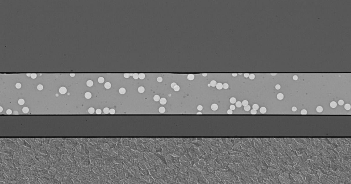 Figure 5: A cross-sectional SEM image showing a multilayer thin film stack on a silicon substrate, with distinct adhesion, functional nanocomposite, and protective coating layers visible.
Coating Method Selection Guide
| Method | Thickness | Conformality | Materials | Substrate | Best For |
| CVD | 10nm-10um | Excellent | Oxides, Nitrides | Si, Metal | Semiconductors |
| PVD | 10nm-5um | Line-of-sight | Metals, Ceramics | Si, Glass | Hard coatings |
| ALD | 1nm-100nm | Perfect | Oxides, Metals | Complex 3D | Precise control |
| Sol-gel | 50nm-10um | Good | Oxides, Hybrids | Any | Large area |
| Spray | 100nm-50um | Good | Nanocomposites | Any size | Rapid coating |
| Dip coat | 20nm-1um | Excellent | Oxides, Polymers | 3D shapes | Optical lenses |
Characterization and Quality Assurance
Every coating development project includes comprehensive characterization to verify that the deposited film meets the specified functional requirements. Our analytical capabilities encompass:
- Thickness measurement by spectroscopic ellipsometry, profilometry, and cross-sectional SEM, with technique selection based on film thickness range and substrate transparency
- Surface morphology and roughness by atomic force microscopy and scanning electron microscopy, quantifying root-mean-square roughness from sub-nanometer to micrometer scales
- Chemical composition and bonding state by X-ray photoelectron spectroscopy, energy-dispersive X-ray spectroscopy, and Fourier-transform infrared spectroscopy, verifying stoichiometry and detecting trace contaminants
- Crystallographic structure by X-ray diffraction and transmission electron microscopy, identifying crystalline phases, grain size, and preferred orientation
- Adhesion strength by pull-off testing and cross-hatch tape testing per ASTM D3359, ensuring coating durability under mechanical stress and thermal cycling
- Functional performance testing including contact angle goniometry for hydrophobic coatings, salt spray testing for corrosion resistance, UV-Vis spectroscopy for optical coatings, and four-point probe for conductive films
Application Areas
Our nanomaterial-enhanced coating and film development services address diverse research and industrial needs:
- Aerospace and defense: superhydrophobic anti-icing coatings for aircraft surfaces, transparent conductive coatings for electromagnetic shielding, and wear-resistant coatings for turbine components
- Medical devices: antimicrobial silver nanoparticle coatings, biocompatible ALD barrier layers on implants, and hydrophilic coatings for catheter lubricity
- Electronics and optoelectronics: passivation layers for semiconductor devices, transparent conductive oxide films for touch screens, and anti-reflection coatings for solar cells and display panels
- Automotive: scratch-resistant UV-curable clear coats, hydrophobic self-cleaning paint treatments, and corrosion-resistant underbody coatings
- Energy: anti-reflection coatings for photovoltaic modules, barrier coatings for fuel cell membranes, and catalytic coatings for electrodes in electrochemical energy conversion devices
If you are interested in our products or services, please don't hesitate to contact us.