
Graphene and 2D Material Synthesis Services
Since its isolation in 2004, graphene has catalyzed an entirely new field of materials science. This single-atom-thick sheet of sp2-hybridized carbon atoms exhibits a remarkable combination of properties — electron mobility exceeding 200,000 cm2/Vs, thermal conductivity surpassing 5000 W/mK, mechanical strength 200 times that of steel, and an enormous specific surface area of 2630 m2/g. These attributes have positioned graphene and the broader family of two-dimensional materials as transformative building blocks for next-generation electronics, energy systems, composites, and biomedical technologies.
At Eata Nanomaterials, we provide end-to-end synthesis and functionalization services for graphene and a comprehensive range of 2D materials. Our capabilities span bottom-up growth via chemical vapor deposition, top-down exfoliation of bulk crystals, wet chemical synthesis of graphene oxide and reduced graphene oxide, and the selective etching protocols required for MXene production. Every material we deliver is accompanied by rigorous characterization data confirming layer number, defect density, lateral dimensions, and surface chemistry — ensuring you receive exactly what your research requires.
Graphene Synthesis: CVD, Exfoliation & Nanoplatelets
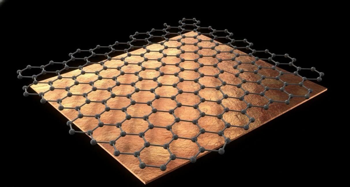 Figure 1: Monolayer graphene with honeycomb hexagonal carbon lattice structure on copper substrate
The quality and properties of graphene are profoundly influenced by the synthesis method employed. We offer multiple production pathways, each optimized for different applications and performance requirements. Chemical vapor deposition (CVD) on copper or nickel substrates produces large-area, high-quality graphene films with low defect densities ideal for electronic and optoelectronic devices. Liquid-phase exfoliation and mechanical exfoliation yield discrete graphene flakes suitable for composite reinforcement, conductive inks, and energy storage applications.
Our few-layer graphene (FLG) and graphene nanoplatelet (GNP) products occupy a particularly important niche in the 2D materials landscape. FLG comprises 3-10 stacked graphene layers according to ISO/TS 80004-13, offering a pragmatic balance between the extraordinary properties of monolayer graphene and the processability required for industrial-scale applications. GNPs provide even greater thickness while retaining high aspect ratios that deliver exceptional mechanical and electrical reinforcement in composite matrices.
Graphene synthesis capabilities:
- CVD graphene on Cu/Ni: Low-pressure CVD at 900-1050 degrees C using CH4 precursors; monolayer to few-layer control via growth time and methane partial pressure; grain sizes up to millimeters; sheet resistance 2000-6000 ohm/sq for monolayer.
- Liquid-phase exfoliation: Sonication-assisted exfoliation of graphite in NMP, DMF, or aqueous surfactant solutions; scalable production of few-layer graphene with lateral dimensions tunable from 100 nm to several microns.
- Graphene nanoplatelets: Wet jet milling and thermal exfoliation of intercalated graphite; thickness 5-15 nm, lateral size 1-50 um, surface area 50-350 m2/g; ideal for polymer nanocomposites and conductive coatings.
- Electrochemical exfoliation: Anodic or cathodic electrochemical intercalation and expansion of graphite foils; rapid, environmentally friendly production of high-quality few-layer graphene dispersions.
- Epitaxial graphene on SiC: High-temperature vacuum annealing (>1400 degrees C) of silicon carbide substrates for wafer-scale electronic-grade graphene with excellent carrier mobility.
Graphene Oxide & Reduced Graphene Oxide Synthesis
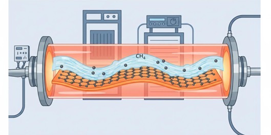 Figure 2: Chemical vapor deposition process showing methane decomposition and graphene self-assembly on heated copper foil in a quartz tube furnace
Graphene oxide (GO) and its chemically or thermally reduced counterpart (rGO) represent the most widely processed forms of graphene in both research and commercial applications. The oxygen-containing functional groups — hydroxyl, epoxy, and carboxyl — that decorate GO sheets render them hydrophilic and dispersible in water and polar organic solvents, a crucial advantage over pristine graphene for solution-phase processing. These same functional groups provide reactive handles for chemical functionalization, biomolecule conjugation, and polymer grafting.
Our GO synthesis follows the modified Hummers' method with rigorous control over oxidation degree, flake size, and purity. The extent of oxidation directly determines the balance between dispersibility and electrical conductivity, and we fine-tune this parameter to match your application. For rGO, we offer multiple reduction pathways — chemical reduction using ascorbic acid, hydrazine, or sodium borohydride; thermal annealing at 300-1100 degrees C under inert atmosphere; and electrochemical reduction — each yielding materials with distinct C/O ratios, defect structures, and electronic properties.
GO and rGO customization options:
- Oxidation degree control: Hummers' method with tunable KMnO4 ratios and reaction times to achieve C/O ratios from 1.5 to 4.0, balancing hydrophilicity against electronic conductivity.
- Flake size selection: Centrifugation-based size fractionation yielding small (50-200 nm), medium (200-500 nm), and large (>500 nm) GO sheets for targeted applications.
- Reduction method optimization: Green chemical reduction, thermal reduction, electrochemical reduction, or solvothermal reduction — selected based on required conductivity, defect tolerance, and processing constraints.
- Dispersion formulation: Concentrated aqueous or organic solvent dispersions at 1-20 mg/mL with surfactant stabilization or solvent-exchange processing.
Transition Metal Dichalcogenide & h-BN Synthesis
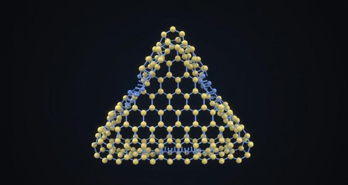 Figure 3: Monolayer MoS2 triangular nanosheet showing molybdenum atoms sandwiched between two sulfur layers in hexagonal crystalline structure
Beyond graphene, the broader family of 2D layered materials offers an expanding palette of electronic, optical, and chemical properties. Transition metal dichalcogenides (TMDs) such as MoS2, WS2, MoSe2, and WSe2 are semiconductors with layer-dependent bandgaps that transition from indirect (~1.2-1.8 eV in bulk) to direct (~1.8-2.1 eV in monolayer), making them exceptional candidates for transistors, photodetectors, and catalysis. Hexagonal boron nitride (h-BN) serves as an atomically flat, wide-bandgap dielectric that is electrically insulating yet shares graphene's hexagonal lattice structure, making it the ideal substrate and encapsulant for van der Waals heterostructures.
We synthesize TMDs and h-BN through both bottom-up CVD growth and top-down liquid-phase exfoliation approaches. CVD enables production of large-area, high-crystallinity monolayer and few-layer films on diverse substrates, while exfoliation provides dispersions of discrete nanosheets suitable for solution processing, composite formulation, and energy device fabrication.
| Material | Synthesis Method | Key Properties & Applications |
| MoS2 | CVD on SiO2/Si; LPE in NMP/water | Direct bandgap 1.8 eV (monolayer); photocatalysis, transistors, sensors |
| WS2 | CVD on sapphire; LPE | Larger exciton binding energy; stronger photoluminescence than MoS2 |
| MoSe2 / WSe2 | CVD; LPE; MBE | Smaller bandgap than sulfides; NIR photodetection, tunneling devices |
| h-BN | LPCVD on Cu/Ni; MBE | Wide bandgap ~5.9 eV; atomically flat dielectric; thermal conductor |
| Black phosphorus | Mechanical exfoliation; LPE | Tunable bandgap 0.3-2.0 eV; high carrier mobility; anisotropic properties |
| NbS2 / TaS2 | CVD; chemical transport | Metallic and superconducting phases; charge density wave materials |
MXene Synthesis & Surface Engineering
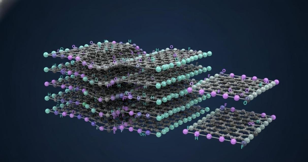 Figure 4: Ti3C2Tx MXene nanosheet with surface termination groups including hydroxyl, fluorine, and oxygen, showing accordion-like exfoliated morphology
MXenes represent one of the most exciting frontiers in the 2D materials landscape. These transition metal carbides, nitrides, and carbonitrides — produced by selectively etching the A-group element layers from MAX phase precursors — combine metallic conductivity with hydrophilic surfaces, making them uniquely suited for energy storage, electromagnetic interference shielding, sensors, and biomedical applications. Since the first report of Ti3C2Tx in 2011, the MXene family has expanded to over 30 compositions with tailored properties.
Our MXene synthesis service employs both HF-based and fluoride-salt-based (LiF/HCl, MIN etching) methods to produce delaminated, few-layer MXene dispersions. The surface termination groups (-OH, -F, -O) introduced during etching profoundly influence electrochemical performance, dispersibility, and chemical reactivity. We control etchant composition, temperature, and post-processing to optimize these surface terminations for your target application.
MXene synthesis portfolio:
- Ti3C2Tx: The most widely studied MXene; selective etching of Ti3AlC2 MAX phase; metallic conductivity ~4600 S/cm; applications in energy storage, EMI shielding, and photothermal therapy.
- Ti2CTx: Lighter MXene with larger interlayer spacing; higher specific capacity for battery and supercapacitor electrodes.
- Nb2CTx / V2CTx: Early transition metal MXenes with distinct electronic structures; promising for catalysis and sensing applications.
- Mo2CTx: Double-transition-metal MXene from Mo2Ga2C precursors; unique catalytic properties for hydrogen evolution reaction.
- Delamination & processing: Intercalation with Li+, TMA+, or DMSO followed by mild sonication; size fractionation via centrifugation; stable aqueous dispersions at 5-50 mg/mL.
2D Material Surface Functionalization & Integration
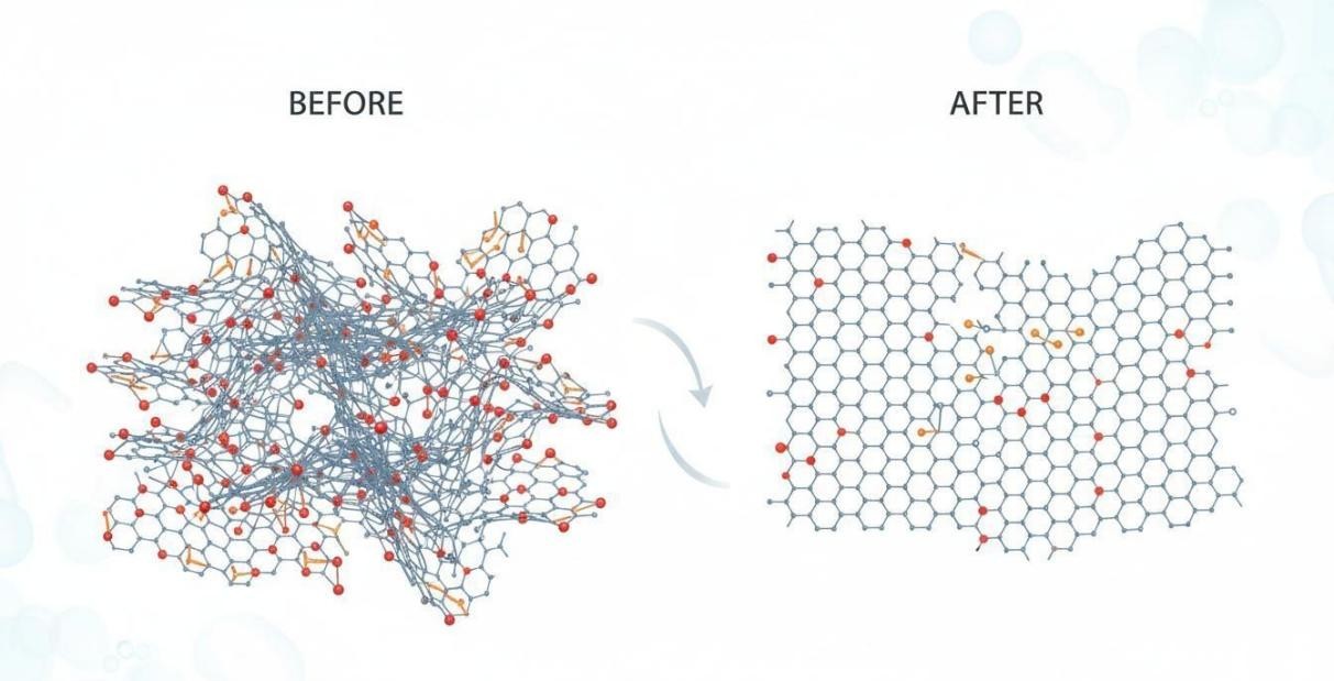 Figure 5: Graphene oxide sheets undergoing reduction to restore sp2 carbon network, showing removal of oxygen functional groups and recovery of electronic conductivity
As-synthesized 2D materials frequently require surface modification to achieve compatibility with target matrices, enable specific molecular recognition, or introduce responsive behaviors. Our surface functionalization service transforms pristine 2D materials into application-ready building blocks through covalent and non-covalent modification strategies that preserve the intrinsic properties of the underlying nanosheet.
For graphene and GO, we leverage the rich surface chemistry of oxygen functional groups and the pi-electron cloud of the sp2 carbon lattice. TMD surfaces expose transition metal edges and chalcogen basal planes that serve as distinct reactive sites. MXene surfaces present a mixture of -OH, -F, and =O terminations that can be exchanged and modified to tune electrochemical and chemical behavior. Each material class demands a tailored functionalization strategy, and our chemists have developed optimized protocols for the full range of 2D material platforms.
| Functionalization | Description |
| Covalent modification | Carbodiimide coupling, silanization, diazonium grafting, click chemistry on GO/MXene; introduces stable chemical linkages for bioconjugation and polymer attachment |
| Non-covalent functionalization | Pi-pi stacking with pyrene derivatives; hydrophobic interaction with surfactants; electrostatic binding with polyelectrolytes; preserves pristine electronic structure |
| Polymer grafting | PEGylation for stealth properties; PVA, PDMA, chitosan for biocompatibility and enhanced dispersion; controlled brush density and chain length |
| Biomolecule conjugation | Antibody, peptide, aptamer, and enzyme attachment for biosensing and targeted delivery; fluorescent protein and DNA conjugation |
| Doping & heteroatom incorporation | Nitrogen, boron, sulfur doping of graphene and TMDs via CVD or thermal treatment; tunes electronic structure and catalytic activity |
Comprehensive 2D Material Characterization
Accurate characterization is indispensable for quality control, process optimization, and meaningful research with 2D materials. Every batch of material synthesized at Eata Nanomaterials undergoes rigorous analytical assessment to confirm structural integrity, layer number, lateral dimensions, chemical composition, and defect density. We provide detailed characterization reports with all raw data, enabling direct inclusion in publications and grant applications.
- Structural characterization: Raman spectroscopy (G, D, 2D band analysis for layer number and defect density); X-ray diffraction (002 peak position and width for interlayer spacing); atomic force microscopy (direct thickness measurement with sub-nanometer resolution); transmission electron microscopy (lattice imaging, SAED patterns, and edge counting).
- Chemical analysis: X-ray photoelectron spectroscopy (elemental composition, oxidation states, C/O ratio); Fourier-transform infrared spectroscopy (functional group identification); energy-dispersive X-ray spectroscopy (elemental mapping at nanoscale); inductively coupled plasma mass spectrometry (trace metal quantification).
- Morphological assessment: Scanning electron microscopy (flake size, morphology, dispersion quality); dynamic light scattering (hydrodynamic size in dispersions); specific surface area by BET nitrogen adsorption; thermal gravimetric analysis (thermal stability and functional group decomposition profiles).
- Electronic & optical properties: UV-Vis absorption spectroscopy (bandgap determination for TMDs, plasmon resonance for graphene); photoluminescence spectroscopy (direct bandgap emission from monolayer TMDs); Hall effect measurement (carrier density and mobility); four-point probe (sheet resistance of thin films).
Application-Driven 2D Material Development
The remarkable versatility of 2D materials stems from the ability to tune their properties through synthesis conditions, layer number, defect engineering, and surface modification. We collaborate closely with clients to develop application-specific materials that address real-world challenges across electronics, energy, healthcare, and advanced materials sectors.
- Energy storage & conversion: High-surface-area MXenes and TMDs for supercapacitor electrodes and battery anodes; heterostructure engineering for photocatalytic water splitting; graphene-based conductive additives for enhanced rate capability.
- Electronics & photonics: CVD graphene for transparent conductive electrodes and field-effect transistors; h-BN as gate dielectric and encapsulant; MoS2 for flexible and low-power logic devices.
- Biomedical applications: GO and rGO for drug delivery, photothermal therapy, and biosensing; surface-engineered MXenes for antimicrobial coatings and cancer theranostics; fluorescent TMD quantum dots for bioimaging.
- Composite materials: GNP and FLG reinforced polymer, metal, and ceramic matrix composites; EMI shielding formulations; thermally conductive adhesives and coatings.
- Environmental remediation: GO membranes for water purification and desalination; MoS2 and WS2 for heavy metal ion adsorption; photocatalytic 2D materials for pollutant degradation.
Access the Full Potential of 2D Materials for Your Research
Contact Eata Nanomaterials to discuss your graphene and 2D material synthesis requirements. Whether you need monolayer CVD graphene, delaminated MXenes, functionalized TMDs, or application-specific rGO, our materials scientists will develop a tailored synthesis and characterization program to advance your project.