

Products
- High-Quality Graphene
- CVD Graphene, Graphene-Like Materials
- Graphene-Like Series
- Defect-Free Single-Crystal Graphene and Graphene-Like Materials (Mechanical Exfoliation)
- Quantum Dot Series
- Aggregation-Induced Emission (AIE)
- Near-Infrared II (NIR-II) Fluorescent Dyes
- Graphdiyne
- Two-Dimensional Transition Metal Carbides/Nitrides/Borides (MXene)
- Metal Nanomaterials and Other Functional Bio-Nanomaterials
- Metal-Organic Frameworks (MOF)
- Covalent Organic Frameworks (COF)
- Two-Dimensional Layered Metal Oxides (LDH)
- Carbon Nanotube Powders, Pastes
- Carbon Nanotube Arrays and Special Carbon Nanotube Materials
- High-Quality Metallic and Semiconducting High-Purity Single-Walled Carbon Nanotubes
- Carbon Nanotube Sponges
- Mesoporous Carbon and Carbon Nanomaterials
- High-Quality Fullerenes
- One-Dimensional Nanomaterials
- Molecular Sieves
- Inorganic Nanomaterials
- Perovskite Materials
- Highly Oriented Pyrolytic Graphite (HOPG)
- Organic Materials
- Single-Atom Catalysts
- Thermoelectric Materials
- Sodium Storage Materials
- Industrial-Grade Nanomaterials
- Solid-State Lithium Batteries
- Hydrogel Series and Consumables
Online Inquiry
High-Quality Metallic and Semiconducting High-Purity Single-Walled Carbon Nanotubes
Rolled from a single sheet of graphene into seamless hollow cylinders roughly one nanometer in diameter, single-walled carbon nanotubes occupy a unique position in the nanomaterials landscape. Their electronic character — whether they conduct electricity like a metal or behave as a semiconductor with a tunable bandgap — depends entirely on how the graphene sheet is rolled, a geometric parameter known as chirality or the chiral index (n, m). Armchair configurations uniformly exhibit metallic behavior, while the vast majority of possible rollings produce semiconducting tubes with bandgaps inversely proportional to their diameter. In as-grown material, roughly one-third of tubes are metallic and two-thirds semiconducting, all intermixed in a tangled assortment that must be untangled before high-performance devices can be built.
Eata Nanomaterials has developed and refined a suite of postsynthetic separation techniques to isolate electronic species with purities exceeding 99%. Through density gradient ultracentrifugation, temperature-controlled gel chromatography, and aqueous two-phase extraction, we enrich metallic and semiconducting populations from raw arc discharge, HiPco, CoMoCAT, and laser ablation feedstock. The resulting products arrive at your laboratory as individualized, surfactant-stabilized aqueous dispersions or as thin films deposited on substrates of your choice — characterization data included with every shipment. Whether you are fabricating field-effect transistors, transparent conductors, or near-infrared photodetectors, our sorted SWCNTs provide the electronic monodispersity that unpurified material simply cannot match.
Metallic Single-Walled Carbon Nanotubes
Metallic SWCNTs function as genuine one-dimensional conductors where electrons travel ballistically over micrometer distances without scattering. Their atomically smooth surfaces support current densities orders of magnitude higher than copper, while their mechanical flexibility allows them to bend and twist without the fatigue that plagues metal wires. These attributes have propelled metallic nanotubes to the forefront of research in high-frequency interconnects, transparent electrodes, and electrochemical sensor platforms.
Our metallic-enriched products are isolated from raw SWCNT mixtures through selective adsorption on allyl dextran-based gels followed by controlled desorption, yielding fractions with metallic purities routinely exceeding 99% as verified by Raman spectroscopy and optical absorbance. Available diameters range from 0.8 nm for small-diameter HiPco-derived material to 1.7 nm for large-diameter arc discharge populations. We supply metallic SWCNTs as aqueous dispersions stabilized with sodium dodecyl sulfate (SDS) or sodium cholate, as spray-coated films on glass or PET, or as dry powders after surfactant removal upon request.
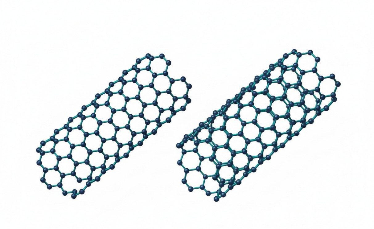 Atomic structures of single-walled carbon nanotubes showing metallic armchair and semiconducting zigzag configurations
Semiconducting Single-Walled Carbon Nanotubes
Semiconducting SWCNTs possess direct bandgaps that span the near-infrared to mid-infrared range depending on diameter — a property unmatched by any conventional semiconductor material. Their lack of surface dangling bonds eliminates the trap states that plague silicon and III-V devices, enabling exceptionally high carrier mobility and near-ideal subthreshold slopes in field-effect transistor configurations. When assembled into densely aligned films at purities approaching 99.9999%, semiconducting nanotubes deliver on-current densities and switching speeds competitive with silicon CMOS, but at substantially lower operating voltages and with inherent flexibility.
Eata Nanomaterials offers semiconducting SWCNT fractions sorted by electronic type and further refined by diameter through density gradient ultracentrifugation. Our standard catalog includes high-purity semiconducting material derived from arc discharge (diameter ~1.4 nm and ~1.6 nm), HiPco (diameter 0.8–1.2 nm), and CoMoCAT (diameter 0.7–0.9 nm) feedstock, with optical bandgaps spanning 0.55 eV to 1.1 eV. Each batch ships with absorbance spectra, Raman I_D/I_G ratios, and purity estimates based on the intensity ratio of the metallic M11 peak to the semiconducting S22 peak.
 Glass vials containing sorted single-walled carbon nanotube dispersions of different chiralities and electronic types, showing characteristic color variations
Separation Technology: From Mixture to Monodispersity
The challenge of separating nanotubes by electronic type hinges on exploiting subtle differences in how metallic and semiconducting tubes interact with surfactants, gels, and solvent systems. Density gradient ultracentrifugation (DGU) exploits the fact that SDS-wrapped metallic and semiconducting tubes possess slightly different buoyant densities in aqueous iodixanol gradients. Following hours of ultracentrifugation at 150,000 g or greater, the two populations resolve into visually distinct colored bands that can be extracted individually. DGU excels at simultaneously sorting by electronic type and refining diameter distributions, delivering the tightest monodispersity of any available technique.
Gel chromatography offers a more scalable pathway. When SDS-dispersed SWCNTs pass through a column packed with allyl dextran-based gel, semiconducting species adsorb preferentially to the gel surface through stronger van der Waals interactions with the dextran matrix, while metallic species elute first. Raising the temperature sharpens these differential interactions, enabling single-chirality separation in a single step — seven distinct (n, m) species have been isolated from HiPco feedstock using temperature-controlled gel chromatography in our partner laboratories. For applications demanding the highest throughput at moderate purity, aqueous two-phase extraction using polyethylene glycol and dextran systems provides a rapid, low-cost route to 95%+ semiconducting enrichment.
 Density gradient ultracentrifugation tube showing separated bands of metallic and semiconducting single-walled carbon nanotubes
Field-Effect Transistors and Beyond
Semiconducting SWCNT thin-film transistors have matured from laboratory curiosities into serious contenders for beyond-silicon electronics. Wafer-scale deposition of densely aligned nanotube films yields devices with channel lengths down to 50 nm, on/off ratios exceeding 10^6, and carrier mobilities surpassing 100 cm^2 V^-1 s^-1 — all at processing temperatures compatible with back-end-of-line integration on existing CMOS wafers. Ferroelectric gate dielectrics have further demonstrated reconfigurable p-type and n-type operation from a single device, suggesting a path toward polarity-controllable logic that silicon cannot replicate.
Metallic SWCNTs complement their semiconducting counterparts as source/drain contacts and interconnects in nanotube integrated circuits. Their all-carbon composition eliminates Schottky barrier formation at metal-semiconductor junctions, reducing contact resistance and improving current injection efficiency. The absence of electromigration failure modes seen in copper interconnects positions metallic nanotubes as a long-term replacement for on-chip wiring in aggressively scaled technology nodes.
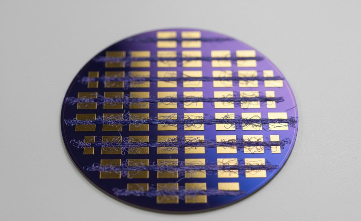 Silicon wafer patterned with arrays of single-walled carbon nanotube field-effect transistor devices featuring gold electrode contacts
Flexible and Transparent Electronics
Perhaps the most commercially immediate application of sorted SWCNTs lies in flexible, transparent conducting films. Networks of metallic-enriched nanotubes deposited from solution achieve sheet resistances below 100 ohm per square at 90% optical transmittance, matching the performance of indium tin oxide while surviving thousands of bending cycles around millimeter-radius mandrels. These films already appear in prototypes of foldable displays, stretchable health monitors, and conformal antennas.
Semiconducting SWCNT networks enable the active switching layers in flexible thin-film transistor backplanes for OLED displays and e-paper, operating at voltages low enough for portable battery-powered devices. Photodet arrays fabricated from chirality-sorted tubes extend sensitivity into the short-wave infrared, opening biomedical imaging and night-vision applications inaccessible to silicon-based sensors. Whatever the platform — rigid silicon, flexible polymer, or stretchable elastomer — our sorted SWCNTs integrate through room-temperature solution processing that preserves substrate integrity.
 Flexible transparent electronic device using single-walled carbon nanotube thin film wrapped around a cylindrical glass substrate
Featured Products
| Products | Specifications | Applications |
| Metallic SWCNT | Purity > 99%; Diameter 0.8–1.7 nm | Interconnects, transparent electrodes |
| Semiconducting SWCNT | Purity > 99–99.9999%; Bandgap 0.55–1.1 eV | FETs, photodetectors, sensors |
| SWCNT DGU sorted | Diameter-refined; Electronic-type enriched | Fundamental research, devices |
| Single-chirality SWCNT | (6,5), (7,5), (7,6), (8,6), (8,4) | NIR optoelectronics, spectroscopy |
| Arc discharge SWCNT | Diameter 1.2–1.7 nm; High crystallinity | High-performance electronics |
| HiPco SWCNT | Diameter 0.8–1.2 nm; Small diameter | FETs, quantum devices |
| CoMoCAT SWCNT | Diameter 0.7–0.9 nm; (6,5) enriched | NIR fluorescence, sensors |
| SWCNT thin film | Aligned network; On/off > 10^6 | Flexible electronics, displays |
Application Landscape
Field-Effect Transistors: High-purity semiconducting SWCNTs serve as the channel material in low-power, high-mobility FETs for logic and memory applications, with demonstrated compatibility with CMOS back-end processing.
Transparent Conductive Films: Metallic SWCNT networks replace ITO in flexible displays, touch screens, and solar cells, offering comparable conductivity with superior mechanical resilience.
Near-Infrared Photodetectors: Diameter-sorted semiconducting tubes with bandgaps in the 0.7–1.3 eV range detect short-wave infrared light for biomedical imaging, environmental monitoring, and optical communications.
Electrochemical Sensors: The high surface area and fast electron transfer kinetics of metallic SWCNT microelectrodes enable sensitive detection of glucose, neurotransmitters, and DNA at nanomolar concentrations.
Interconnects and Wiring: Ballistic conduction in metallic SWCNTs supports current densities exceeding 10^9 A/cm^2, offering a pathway to replace copper in sub-5 nm technology nodes without electromigration failure.
Photovoltaic Devices: Semiconducting SWCNTs function as both light absorbers and charge transport channels in organic and hybrid solar cells, with power conversion efficiencies steadily approaching commercial viability.
Characterization and Quality Assurance
Each batch of sorted SWCNT material undergoes a comprehensive analytical protocol before release. Optical absorbance spectroscopy identifies the presence and relative intensity of the S11, S22, M11, and M22 transitions, providing a quantitative estimate of electronic-type purity. Raman spectroscopy with resonant excitation at multiple wavelengths (532 nm, 633 nm, 785 nm) confirms diameter distribution and structural quality through the radial breathing mode frequency and I_D/I_G intensity ratio. Thermogravimetric analysis quantifies residual metal catalyst content, typically below 1 wt% in our purified products. For thin-film products, four-point probe measurements report sheet resistance, and atomic force microscopy documents network density and morphology. We provide these data sheets with every order at no additional charge.
Tailored Enrichment and Custom Synthesis
Standard catalog items represent only a starting point. We regularly engage in collaborative projects that push beyond off-the-shelf offerings: single-chirality isolation of specific (n, m) species for fundamental optical studies, selective removal of surfactant residues through solvent exchange and dialysis for applications where contamination must be minimized, deposition of sorted nanotubes onto customer-supplied substrates with controlled alignment by dielectrophoresis or Langmuir-Blodgett assembly, and covalent functionalization of tube sidewalls or end-groups to enhance dispersion stability or introduce specific chemical reactivity. If your project demands a nanotube population with a particular diameter, chirality, electronic character, or surface chemistry, our team is prepared to design a separation and processing protocol around your specifications.
Request a Quote— Contact Eata Nanomaterials to discuss your metallic or semiconducting SWCNT requirements, request product samples, or explore a custom separation and processing engagement.
| Catalog Number | Product Name | Order | Quantity |
|---|---|---|---|
| SHSCN-0001 | Semiconducting Single-Walled Carbon Nanotube Solution 99.9% (semiconductor) |
-
+
|
|
| SHSCN-0002 | Large Diameter Semiconducting Single-Walled Carbon Nanotube Solution 99.9% |
-
+
|
|
| SHSCN-0003 | Small Diameter Semiconducting Single-Walled Carbon Nanotube Solution 99.9% |
-
+
|
|
| SHSCN-0004 | Metallic Single-Walled Carbon Nanotube Solution 98% (metallic) |
-
+
|
|
| SHSCN-0005 | Semiconducting Single-Walled Carbon Nanotube Solution |
-
+
|
|
| SHSCN-0006 | Semiconducting Single-Walled Carbon Nanotube Solution 95% (semiconductor) |
-
+
|
|
| SHSCN-0007 | Small Diameter Metallic Single-Walled Carbon Nanotube Solution 95% |
-
+
|
|
| SHSCN-0008 | Dielectric Ink for Printed Electronics |
-
+
|
|
| SHSCN-0009 | Semiconducting SWCNT + Dielectric Ink Set for Printed TFT |
-
+
|
|
| SHSCN-0010 | Multi-Walled Carbon Nanotube Powder 95% 10-20 nm |
-
+
|
For Research or Industrial Raw Materials, Not For Personal Medical Use!