

Morphological and Structural Characterization Services
Understanding the morphological and structural attributes of nanomaterials forms the cornerstone of successful research. Size, shape, crystallinity, surface area, and aggregation state directly govern optical, electronic, magnetic, catalytic, and biological behaviors. Without rigorous characterization, even the most elegantly synthesized nanomaterials remain incompletely understood and poorly reproducible.
At Eata Nanomaterials, we operate a state-of-the-art analytical facility equipped with advanced microscopy, diffraction, and spectroscopic instrumentation. Our characterization services span direct imaging techniques that visualize individual particles, ensemble methods that probe bulk structural properties, and surface-sensitive approaches that decode interfacial chemistry. Every measurement is performed by experienced analysts who understand the unique challenges of nanoscale sample preparation and data interpretation.
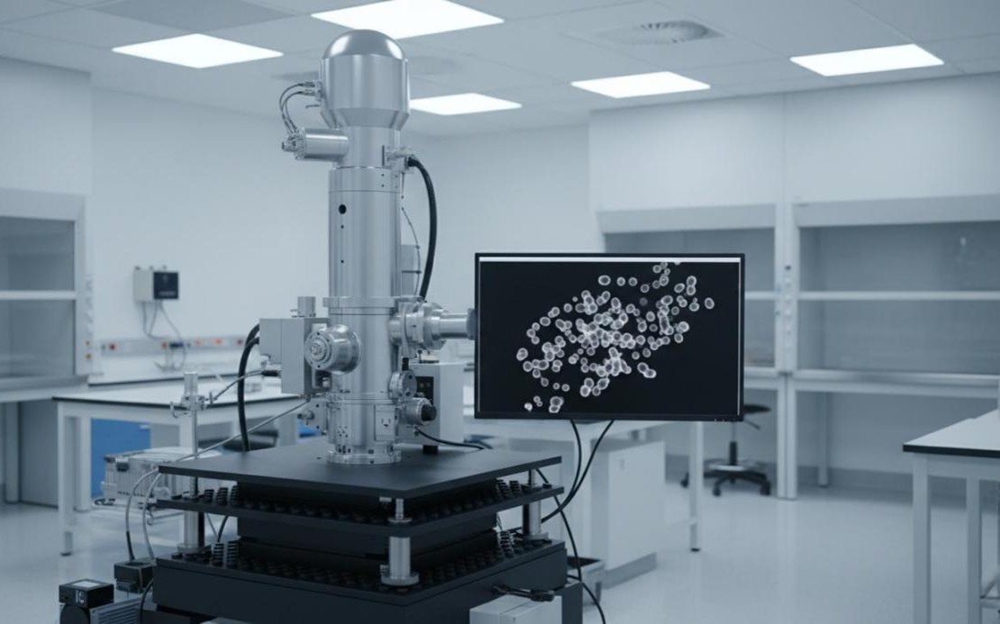 Figure 1: A transmission electron microscope system with specimen column and monitor displaying nanoparticle images.
Electron Microscopy: Direct Visualization at the Nanoscale
Electron microscopy provides the most direct and information-rich approach to nanomaterial morphological characterization. By harnessing the sub-angstrom wavelength of accelerated electrons, these techniques resolve features far below the diffraction limit of light, revealing particle dimensions, geometries, internal structures, and elemental compositions with exceptional clarity.
Transmission Electron Microscopy (TEM): Our TEM platform achieves spatial resolution from the atomic level to the micrometer scale, making it the definitive method for nanoparticle characterization. TEM reveals particle size distribution, shape uniformity, aspect ratio, aggregation state, and crystallographic structure through direct imaging. High-resolution TEM (HRTEM) resolves interplanar spacings and lattice orientations, enabling phase identification and defect analysis. Selected area electron diffraction (SAED) patterns distinguish single-crystal from polycrystalline domains and quantify orientation distributions. We also offer energy-dispersive X-ray spectroscopy (EDX) mapping for elemental composition analysis with nanometer spatial resolution.
Scanning Electron Microscopy (SEM): SEM generates high-resolution topographic images by scanning a focused electron beam across the sample surface and collecting secondary and backscattered electrons. With magnification capabilities reaching 100,000x and exceptional depth of field, SEM excels at characterizing particle size distribution, three-dimensional morphology, surface texture, and assembly architectures. Our instrument is equipped with EDX for simultaneous elemental analysis, enabling correlation of morphology with chemical composition. Environmental SEM modes permit imaging of uncoated or hydrated samples without extensive preparation.
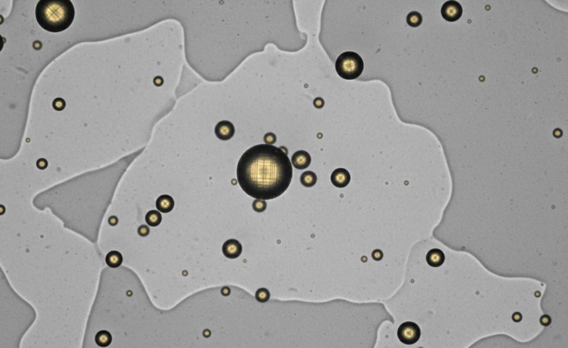 Figure 2: A high-resolution TEM image showing individual nanoparticles with visible crystalline lattice fringes distributed on a carbon support film.
X-Ray Diffraction: Crystallographic Structure and Phase Analysis
X-ray diffraction (XRD) stands as the gold standard for determining the crystallographic structure, phase composition, and crystallinity of nanomaterials. By measuring the angles and intensities of diffracted X-rays, XRD generates a unique fingerprint that identifies crystallographic phases and reveals critical structural parameters.
Our XRD characterization services provide:
- Phase identification by matching measured diffraction patterns against international crystallographic databases (ICDD PDF)
- Crystallite size determination using the Scherrer equation, correlating peak broadening with domain dimensions
- Lattice parameter refinement quantifying unit cell dimensions and detecting strain-induced distortions
- Preferred orientation analysis revealing anisotropic growth patterns in shaped nanocrystals
- Quantitative phase analysis determining the relative abundance of coexisting crystalline phases
XRD is particularly valuable for monitoring synthesis quality, verifying phase purity, and comparing batch-to-batch consistency. For nanomaterials with dimensions below 5 nm, we employ synchrotron-based small-angle X-ray scattering (SAXS) as a complementary technique for probing particle size in solution.
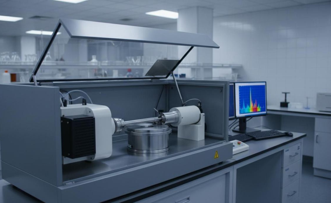 Figure 3: An X-ray diffractometer with goniometer assembly and protective cabinet, with a workstation displaying a diffraction pattern.
Atomic Force Microscopy: Surface Topography and Beyond
Atomic force microscopy (AFM) measures surface topography by rastering a sharp probe tip across the sample surface and recording tip-sample interactions. Unlike electron microscopy, AFM requires no vacuum and operates under ambient, liquid, or controlled atmosphere conditions, enabling characterization of samples in their native state.
Our AFM capabilities extend far beyond simple height mapping:
- Three-dimensional topographic imaging with sub-nanometer height resolution, revealing surface roughness, particle height profiles, and lateral dimensions
- Phase imaging distinguishing materials with different mechanical properties, useful for mapping polymer coatings or composite structures
- Kelvin probe force microscopy (KPFM) mapping surface potential variations across heterogeneous nanomaterial surfaces
- Conductive AFM (C-AFM) measuring local electrical conductivity with nanometer spatial resolution
- Force spectroscopy quantifying adhesion, elasticity, and binding forces between the AFM tip and sample surface
Dynamic and Static Light Scattering
Light scattering techniques provide rapid, non-destructive measurement of particle size distributions in liquid suspension, capturing the hydrodynamic behavior of nanoparticles as they exist in their functional environment.
Dynamic Light Scattering (DLS) analyzes temporal fluctuations in scattered light intensity caused by Brownian motion of particles. Through the Stokes-Einstein relationship, DLS converts diffusion coefficients into hydrodynamic diameter distributions. Results include the intensity-averaged size, polydispersity index (PDI) indicating sample homogeneity, and intensity/volume/number distributions.
Nanoparticle Tracking Analysis (NTA) complements DLS by directly visualizing individual particles through laser-illuminated microscopy, tracking their Brownian motion frame-by-frame. Unlike DLS, NTA resolves polydisperse mixtures and provides particle concentration data alongside size distributions.
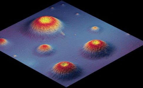 Figure 4: A color-coded 3D AFM topographic image showing spherical nanoparticles on a flat substrate with height variations rendered in warm colors.
Spectroscopic Surface and Chemical Analysis
While microscopy reveals morphology and diffraction exposes structure, spectroscopic techniques decode the chemical composition, oxidation states, and surface functionalization of nanomaterials. These methods provide essential complementary information that completes the characterization picture.
| Technique | Information Provided | Typical Applications |
| XPS | Elemental composition, oxidation states, chemical bonding | Surface chemistry, functional group verification |
| FTIR | Vibrational modes, functional group identification | Organic coating confirmation, ligand analysis |
| Raman | Molecular vibrations, crystal structure, defects | Carbon nanomaterial quality, strain analysis |
| TGA | Thermal stability, organic content, decomposition | Coating quantification, ligand density calculation |
| BET | Specific surface area, pore size distribution | Catalyst evaluation, adsorption capacity |
| Zeta Potential | Surface charge, colloidal stability | Dispersion optimization, aggregation prediction |
Expert Sample Preparation and Data Interpretation
The quality of nanomaterial characterization depends critically on sample preparation. Our experienced team employs specialized protocols tailored to each material class:
- TEM specimen preparation through drop-casting, ultramicrotomy, or focused ion beam (FIB) thinning for cross-sectional analysis
- SEM sample mounting with conductive coatings or low-voltage imaging protocols to minimize charging artifacts
- AFM sample deposition by spin-coating or Langmuir-Blodgett transfer for uniform particle dispersion
- XRD powder specimen preparation ensuring random orientation and optimal packing density
- DLS sample conditioning with controlled sonication, filtration, and equilibration at measurement temperature
Beyond measurement execution, we provide comprehensive data interpretation. Each characterization report includes raw data, processed results with statistical analysis, representative images or spectra, and expert commentary addressing your specific research questions.
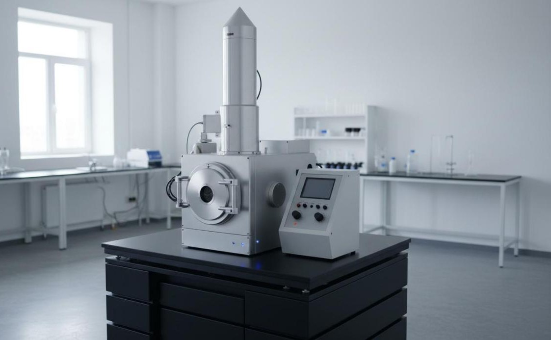 Figure 5: A scanning electron microscope with cubic specimen chamber mounted on a vibration isolation platform in a clean laboratory.
Integrated Multi-Technique Characterization Packages
Individual techniques provide isolated snapshots of nanomaterial properties. Integrated multi-technique characterization builds a comprehensive understanding by combining complementary methods. We offer tailored characterization packages designed around common research needs:
Synthesis Verification Package: TEM + SEM + XRD confirming size, shape, and crystalline phase of newly synthesized nanomaterials
Surface Chemistry Package: XPS + FTIR + Zeta Potential revealing surface functionalization, ligand attachment, and colloidal stability
Drug Delivery Platform Package: DLS + TEM + BET assessing carrier size, morphology, loading capacity, and surface area
Nanocomposite Package: SEM + AFM + XRD mapping filler dispersion, interfacial adhesion, and crystalline structure
Quality Control Package: TEM + XRD + DLS + Zeta for batch-to-batch consistency monitoring
Advance Your Research with Expert Characterization
Whether you require single-technique analysis or comprehensive multi-modal characterization, Eata Nanomaterials delivers precise, reliable data with expert interpretation. Our analytical services are designed to accelerate your research by providing the structural and morphological insights needed to guide synthesis optimization, validate material quality, and publish with confidence.
Submit a service request or contact our analytical team to discuss your specific characterization needs, sample requirements, and recommended techniques.