

Products
- High-Quality Graphene
- CVD Graphene, Graphene-Like Materials
- Graphene-Like Series
- Defect-Free Single-Crystal Graphene and Graphene-Like Materials (Mechanical Exfoliation)
- Quantum Dot Series
- Aggregation-Induced Emission (AIE)
- Near-Infrared II (NIR-II) Fluorescent Dyes
- Graphdiyne
- Two-Dimensional Transition Metal Carbides/Nitrides/Borides (MXene)
- Metal Nanomaterials and Other Functional Bio-Nanomaterials
- Metal-Organic Frameworks (MOF)
- Covalent Organic Frameworks (COF)
- Two-Dimensional Layered Metal Oxides (LDH)
- Carbon Nanotube Powders, Pastes
- Carbon Nanotube Arrays and Special Carbon Nanotube Materials
- High-Quality Metallic and Semiconducting High-Purity Single-Walled Carbon Nanotubes
- Carbon Nanotube Sponges
- Mesoporous Carbon and Carbon Nanomaterials
- High-Quality Fullerenes
- One-Dimensional Nanomaterials
- Molecular Sieves
- Inorganic Nanomaterials
- Perovskite Materials
- Highly Oriented Pyrolytic Graphite (HOPG)
- Organic Materials
- Single-Atom Catalysts
- Thermoelectric Materials
- Sodium Storage Materials
- Industrial-Grade Nanomaterials
- Solid-State Lithium Batteries
- Hydrogel Series and Consumables
Online Inquiry
CVD Graphene, Graphene-Like Materials
At Eata Nanomaterials, we specialize in supplying high-purity CVD graphene and graphene-like two-dimensional (2D) materials tailored for research laboratories, academic institutions, and industrial R&D teams worldwide. Whether you are fabricating next-generation field-effect transistors, building van der Waals heterostructures, or developing advanced composite coatings, our material portfolio is engineered to deliver the structural integrity and electronic performance your project demands.
What Sets Our CVD Graphene Apart
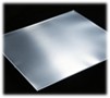
Chemical vapor deposition (CVD) remains the gold-standard technique for producing large-area, high-quality graphene films with tunable layer counts and minimal defect densities. Our roll-to-roll and wafer-scale CVD platforms yield monolayer, bilayer, and few-layer graphene on substrates such as SiO₂/Si, quartz, sapphire, and copper foil—ready for immediate transfer or device integration.
- Monolayer coverage exceeding 98% with Raman 2D/G intensity ratios ≥ 1.5, confirming single-layer uniformity.
- Hall electron mobility up to 4,000 cm²/V·s on SiO₂/Si substrates, enabling high-frequency transistor prototyping.
- Sheet resistance as low as 240–450 Ω/sq (1 cm × 1 cm), competitive with indium tin oxide (ITO) alternatives.
- Grain sizes ranging from ~5 µm (small-grain, high reproducibility) to large-domain films for optoelectronic applications.
- Substrate diameters available up to 6 inches (150 mm), with custom sizing on request.
Graphene-Like 2D Materials Portfolio
Beyond graphene, the 2D materials family unlocks complementary electronic, optical, and thermal properties. We supply transition metal dichalcogenides (TMDCs), hexagonal boron nitride (hBN), and emerging layered compounds grown via CVD or exfoliation methods—each backed by characterization data.
| Material Family | Key Properties | Typical Applications | Available Forms |
| Hexagonal Boron Nitride (h-BN) | Wide band-gap insulator (~5.9 eV); atomically flat surface; excellent thermal stability. | Substrate for graphene devices; tunnel barrier layers; deep-UV emitters. | CVD film on SiO₂/Si or Cu foil; mechanically exfoliated flakes. |
| Molybdenum Disulfide (MoS₂) | Direct band-gap semiconductor (1.8 eV monolayer); high on/off ratio in FETs. | Low-power logic transistors; photodetectors; catalytic hydrogen evolution. | CVD monolayer/multilayer on SiO₂/Si, sapphire, quartz; crystal powder; dispersion. |
| Tungsten Disulfide (WS₂) | Strong spin-orbit coupling; layer-dependent band-gap; high photoluminescence quantum yield. | Valleytronics; flexible optoelectronics; lubricant additives. | CVD film on various substrates; powder; solution. |
| Molybdenum Diselenide (MoSe₂) | Tunable band-gap; good absorption in visible-NIR range; stable in ambient conditions. | Solar cell absorbers; photothermal therapy research; electrocatalysis. | CVD film; mechanically exfoliated monolayer on substrate. |
| Tungsten Diselenide (WSe₂) | Ambipolar transport; high carrier mobility; strong excitonic effects. | CMOS-compatible transistors; quantum dot emitters; flexible sensors. | CVD film; powder; dispersion. |
| Black Phosphorus | Tunable direct band-gap (0.3–2.0 eV); high hole mobility; anisotropic transport. | Mid-infrared photodetectors; anisotropic electronics; thermoelectric devices. | Crystal powder; mechanically exfoliated flakes. |
High-Demand Product Specifications
| Products | Critical Parameters | Typical Use Case |
| Monolayer CVD graphene on SiO₂/Si wafer | Grain size 5–50 µm; 2D/G ≥ 1.5; mobility > 1,500 cm²/V·s | GFET fabrication; biosensor substrates |
| Bilayer CVD graphene film | Bernal stacking; tunable band-gap under electric field; sheet resistance ~500 Ω/sq | Band-gap engineering; tunneling devices |
| Few-layer graphene (3–8 layers) on Cu foil | Thickness 1.0–2.8 nm; transparency 78–90%; conductivity > 10⁴ S/m | Transparent conductive films; EMI shielding |
| Graphene oxide (GO) aqueous dispersion | Concentration 1–10 mg/mL; flake size 0.5–5 µm; C/O ratio ~2:1 | Composite reinforcement; membrane filtration |
| Reduced graphene oxide (rGO) powder | C/O ratio > 8:1; BET surface area 400–600 m²/g; conductivity ~100 S/m | Battery anodes; conductive inks; anti-corrosion coatings |
| hBN film on SiO₂/Si (CVD grown) | Monolayer thickness ~0.33 nm; optical band-gap ~5.9 eV; surface roughness < 0.5 nm | Graphene encapsulation; dielectric substrate |
| Monolayer MoS₂ on sapphire | Domain size up to 100 µm; PL peak ~1.89 eV; FWHM ~45 meV | Photodetector arrays; catalysis research |
| WS₂ monolayer film on SiO₂/Si | Raman E′₂g / A₁g splitting ~21 cm⁻¹; direct band-gap ~2.0 eV | Valley-polarized devices; flexible electronics |
| MoS₂/WS₂/hBN/Graphene heterostructure | Vertically stacked; atomically sharp interfaces; customizable layer sequence | Van der Waals device stacks; quantum transport studies |
| CVD graphene on PET substrate | Flexible; sheet resistance < 350 Ω/sq; transmittance > 85% | Wearable sensors; flexible transparent electrodes |
| Graphene nanoplatelets (GNPs) | Lateral size 1–50 µm; thickness 3–15 nm; bulk conductivity > 500 S/m | Polymer nanocomposites; thermal interface materials |
| TMDC crystal powder (MoS₂, WS₂, WSe₂) | Purity > 99.9%; lateral size 1–10 mm; single-crystal domain | Mechanical exfoliation source; fundamental physics research |
Substrate & Format Flexibility
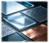
We understand that substrate choice often dictates device yield. That is why we maintain a broad inventory of pre-grown films on the most commonly requested supports, and we offer substrate transfer services for specialized setups.
- Silicon wafers with thermal oxide (SiO₂/Si, 285 nm or 300 nm oxide): the industry standard for back-gated graphene FETs.
- Quartz and sapphire: ideal for optical transmission studies and high-temperature annealing protocols.
- Copper foil and nickel foil: suitable for electrochemical transfer or direct use as current collectors.
- Polyethylene terephthalate (PET) and polyimide (PI): pre-selected for flexible and wearable form factors.
- TEM grids (Cu, Au, or Quantifoil): pre-deposited flakes for immediate electron microscopy analysis.
Tailored Material Solutions — Customization Services
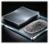
Standard catalog items cover most research needs, yet breakthrough experiments frequently demand bespoke specifications. Our engineering team welcomes custom synthesis requests ranging from single-parameter tweaks to full heterostructure design.
- Layer-count engineering: precise control from monolayer to 10+ layers with intermediate steps.
- Doping and functionalization: nitrogen, boron, or fluorine doping; covalent functionalization for enhanced dispersion.
- Heterostructure assembly: MoS₂/hBN/graphene stacks with rotational alignment (twist-angle) control.
- Patterned growth: selective-area CVD using pre-patterned catalyst films for device-ready geometries.
- Scale-up trials: pilot batches from gram-scale powders to 8-inch wafer films for industrial feasibility studies.
Quality Assurance & Characterization
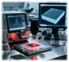
Traceability is non-negotiable in nanomaterial supply. Each shipment includes a batch-specific characterization report summarizing the analytical methods and results relevant to that product line.
- Raman spectroscopy: G, D, and 2D peak positions, FWHM values, and I₂D/I_G ratios for layer identification.
- Atomic force microscopy (AFM): thickness mapping, surface roughness, and coverage percentage.
- Hall-effect measurements: carrier mobility, sheet resistance, and carrier density at room temperature.
- X-ray photoelectron spectroscopy (XPS): elemental composition and C/O ratio quantification for GO/rGO batches.
- Photoluminescence (PL) spectroscopy: peak position and FWHM for TMDC monolayers to confirm direct band-gap quality.
Where Our Materials Are Making an Impact

While we refrain from making unverified performance claims, the following sectors represent the most active research and industrial development areas where our CVD graphene and 2D materials are currently deployed.
- Semiconductor R&D: graphene-based interconnects, TMDC transistors, and tunnel-FET prototypes.
- Energy storage: rGO-enhanced Li-ion battery anodes, supercapacitor electrodes, and solid-state electrolyte interfaces.
- Photonics & optoelectronics: broadband photodetectors, modulators, and transparent conductive electrodes.
- Sensing & detection: electrochemical biosensors, gas sensors, and strain gauges leveraging high surface-to-volume ratios.
- Composite & coating industries: anti-corrosion primers, EMI shielding paints, and thermally conductive polymer blends.
If you are interested in our products or services or have any questions, please feel free to contact us!
| Catalog Number | Product Name | Order | Quantity |
|---|---|---|---|
| GLM-0001 | PET Substrate (20 cm × 30 cm, ~180 μm) |
-
+
|
|
| GLM-0002 | CVD Graphene Film on Copper Substrate (1 cm × 1 cm) |
-
+
|
|
| GLM-0003 | Trivial Transfer Graphene Film (5 cm × 5 cm) |
-
+
|
|
| GLM-0004 | CVD Graphene Film on Copper Substrate (5 cm × 5 cm) |
-
+
|
|
| GLM-0005 | CVD Graphene Growth Copper Foil (20 cm × 30 cm, ~25 μm) |
-
+
|
|
| GLM-0006 | CVD Graphene Film on Copper Foil (2 cm × 2 cm) |
-
+
|
|
| GLM-0007 | CVD Graphene Film on Copper Foil (10 cm × 5 cm) |
-
+
|
|
| GLM-0008 | CVD Graphene Film on Copper Foil (10 cm × 10 cm) |
-
+
|
|
| GLM-0009 | CVD Graphene Film on Copper Foil (15 cm × 10 cm) |
-
+
|
|
| GLM-0010 | CVD Graphene Film on SiO2 Substrate (1 cm × 1 cm) |
-
+
|
For Research or Industrial Raw Materials, Not For Personal Medical Use!