

Products
- High-Quality Graphene
- CVD Graphene, Graphene-Like Materials
- Graphene-Like Series
- Defect-Free Single-Crystal Graphene and Graphene-Like Materials (Mechanical Exfoliation)
- Quantum Dot Series
- Aggregation-Induced Emission (AIE)
- Near-Infrared II (NIR-II) Fluorescent Dyes
- Graphdiyne
- Two-Dimensional Transition Metal Carbides/Nitrides/Borides (MXene)
- Metal Nanomaterials and Other Functional Bio-Nanomaterials
- Metal-Organic Frameworks (MOF)
- Covalent Organic Frameworks (COF)
- Two-Dimensional Layered Metal Oxides (LDH)
- Carbon Nanotube Powders, Pastes
- Carbon Nanotube Arrays and Special Carbon Nanotube Materials
- High-Quality Metallic and Semiconducting High-Purity Single-Walled Carbon Nanotubes
- Carbon Nanotube Sponges
- Mesoporous Carbon and Carbon Nanomaterials
- High-Quality Fullerenes
- One-Dimensional Nanomaterials
- Molecular Sieves
- Inorganic Nanomaterials
- Perovskite Materials
- Highly Oriented Pyrolytic Graphite (HOPG)
- Organic Materials
- Single-Atom Catalysts
- Thermoelectric Materials
- Sodium Storage Materials
- Industrial-Grade Nanomaterials
- Solid-State Lithium Batteries
- Hydrogel Series and Consumables
Online Inquiry
Carbon Nanotube Arrays and Special Carbon Nanotube Materials
At Eata Nanomaterials, we engineer carbon nanotubes into precisely organized arrays and macro-scale architectures that transcend the limitations of conventional powder formats. Through catalytic chemical vapor deposition (CVD) and plasma-enhanced CVD (PECVD), nanotubes self-assemble into vertically oriented forests on silicon wafers, metal foils, and quartz substrates. The resulting structures — dense mats of aligned tubes standing perpendicular to the surface — unlock properties inaccessible in randomly entangled bulk material, from directional thermal conduction and field emission to mechanical drawability and optical transparency.
Our special carbon nanotube portfolio extends well beyond VACNT forests. Double-walled nanotube (DWCNT) arrays merge the electronic finesse of single-walled tubes with the ruggedness of multi-walled ones. Three-dimensional CNT sponges and aerogels boast near-zero density alongside extraordinary elasticity. Continuous fibers and yarns spun directly from forests challenge the mechanical performance of commercial carbon fiber while adding electrical conductivity. Dry-drawn transparent conductive sheets bend and flex where brittle ITO fails. Whatever your application demands — thermal, electrical, mechanical, or optical — we have a nanotube architecture engineered for it.
Patterned VACNT Arrays for Device Integration
Not every application calls for a uniform carpet of nanotubes. Lithographically patterned catalyst islands enable site-specific growth, producing ordered arrays of CNT pillars, pads, and lines with feature sizes from micrometers to millimeters. These patterned architectures serve as individual field emitters in display technology, as microelectrode arrays in biosensing platforms, and as compliant electrical interconnects in flip-chip packaging.
Our photolithography-compatible process deposits catalyst through shadow masks or lift-off patterns, ensuring registry accuracy compatible with semiconductor fabrication workflows. Post-growth, the patterned forests retain their defined geometries without spreading or bridging. We support custom layouts: circular pads for localized emission, rectangular strips for thermal interfaces along specific heat paths, and interdigitated patterns for on-chip supercapacitors. Substrates range from standard 4-inch silicon wafers to flexible polyimide films, accommodating both rigid and bendable device concepts.
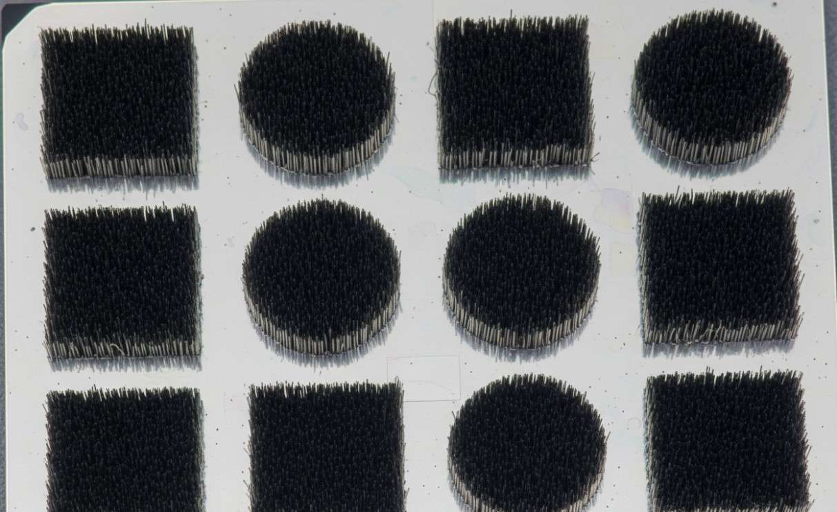 Figure 1: Patterned carbon nanotube arrays with alternating square and circular geometries on a silicon substrate
Superblack CNT Surfaces for Stray-Light Suppression
Dense VACNT forests rank among the most effective light-absorbing materials ever created. When photons enter the forest, they bounce between adjacent nanotube walls in a cascade of internal reflections, losing energy at each encounter until virtually nothing escapes. Measured absorptance exceeds 99.9% across the ultraviolet through far-infrared range — a performance that has made CNT-based coatings the benchmark for stray-light suppression in aerospace and optical instrumentation.
Eata Nanomaterials supplies superblack CNT coatings deposited on aluminum, titanium, and fused silica substrates for use as blackbody references, baffle coatings in telescopes and spectrometers, and calibration targets for remote sensing equipment. The coatings are grown in-house via thermal CVD at temperatures tailored to preserve substrate integrity. For applications requiring mechanical durability, we offer encapsulated versions where a thin permeable overcoat protects the nanotube tips without significantly degrading absorption performance.
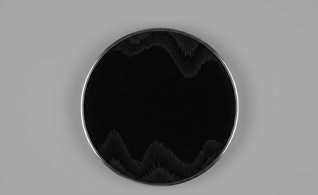 Figure 2: Ultra-black carbon nanotube coating demonstrating near-total light absorption across a circular surface
CNT Thermal Interface Arrays
Thermal management represents one of the most commercially promising roles for VACNT forests. Individual multi-walled nanotubes conduct heat axially at rates approaching 3000 W/mK — comparable to diamond — yet the bulk material remains soft and compliant. When a VACNT forest is sandwiched between a heat-generating chip and a metal heat spreader, the aligned tubes act as microscopic thermal springs, conducting heat efficiently while accommodating thermal expansion mismatches between dissimilar materials.
The resulting thermal interface resistance falls below 10 mm^2 K/W under moderate compression, outperforming conventional thermal greases and phase-change materials while eliminating pump-out and dry-out failures. We supply CNT thermal interface materials as transferable films on carrier substrates, ready to be laminated onto chip surfaces or integrated into power module assemblies. Operating temperatures extend from cryogenic to over 300 C, covering the full range of electronics, photonics, and power semiconductor cooling needs.
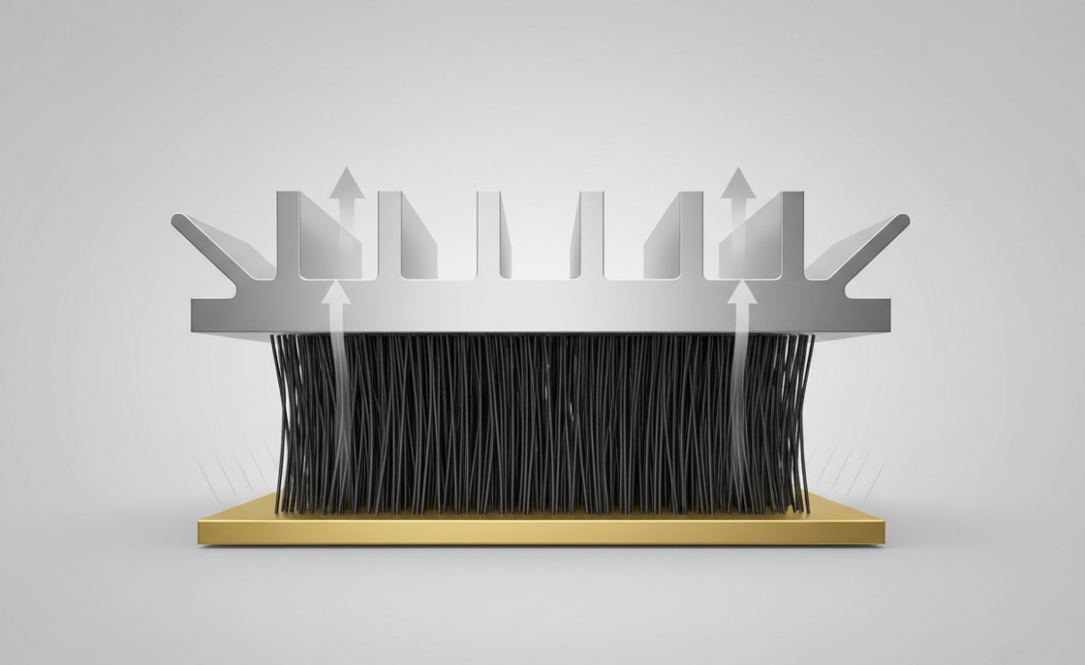 Figure 3: Vertically aligned CNT array bridging between a chip substrate and a metallic heat sink for thermal management
Dry-Drawn Transparent CNT Conductive Sheets
A remarkable property of high-density VACNT forests is their ability to be pulled, like a sheer curtain, into a continuous freestanding sheet. The drawing process aligns nanotubes parallel to the pull direction, creating a thin, flexible film that combines optical transparency with electrical conductivity. Sheet resistances below 200 ohm per square at 85% visible transmittance are routinely achieved, and post-treatment with dopants such as AuCl3 can drive this below 60 ohm per square while maintaining over 90% clarity.
Unlike sputtered indium tin oxide (ITO), CNT sheets bend, fold, and stretch without cracking or delamination. They transfer cleanly onto glass, polymers, textiles, and curved surfaces through simple dry contact printing. We supply these transparent conductive films in rolls or cut sheets for researchers developing next-generation touch panels, flexible displays, wearable sensors, organic photovoltaics, and electrochromic devices. The absence of brittle ceramic components means these electrodes survive thousands of flexing cycles without degradation.
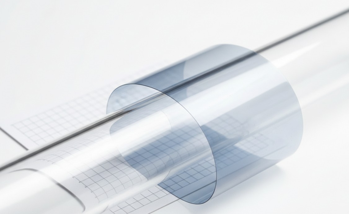 Figure 4: Flexible transparent carbon nanotube conductive film demonstrating optical clarity and bendability
Continuous CNT Fibers and Braided Yarns
Through a process akin to spinning wool from a fleece, nanotube forests can be twisted and drawn into continuous fibers without binders, polymers, or chemical baths. The resulting CNT yarn inherits the exceptional properties of its constituent tubes: tensile strengths reaching several gigapascals, Young's moduli in the hundreds of gigapascals, and electrical conductivities that rival metals on a weight-normalized basis. These fibers can be plied into yarns, woven into fabrics, braided into ropes, or embedded in polymer matrices to create multifunctional composites.
Wet-spinning alternatives disperse nanotubes in surfactant solutions and extrude them through coagulation baths, enabling the incorporation of functional guests — catalysts, pharmaceuticals, or phase-change materials — inside the fiber core. Whether dry-spun or wet-spun, CNT fibers serve as structural reinforcements with built-in sensing capability (resistance changes under strain reveal damage before it becomes critical), as lightweight electrical conductors in aerospace wiring, as Joule heaters that reach hundreds of degrees within seconds, and as artificial muscles that contract under electrical stimulation.
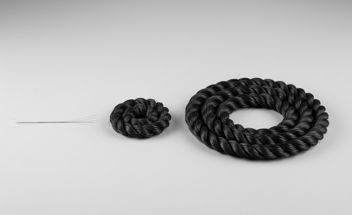 Figure 5: Carbon nanotube fibers, twisted yarns, and braided rope showing hierarchical macroscopic structures
Featured Products
| Products | Specifications | Applications |
| Patterned VACNT array | Feature: 5 um–1 mm; Substrates: Si, quartz, metal | Device integration, biosensors |
| Superblack CNT coating | Absorptance: >99.9% (UV–FIR); CVD grown | Optical calibration, baffles |
| CNT thermal interface | Resistance: <10 mm^2 K/W; Compliance: soft | Power electronics, LEDs |
| Transparent CNT sheet | R_s < 200 ohm/sq; T > 85% at 550 nm | Flexible displays, solar |
| CNT fiber/yarn | Strength: 1–3 GPa; sigma_e: 10^4–10^5 S/m | Composites, smart textiles |
| CNT sponge/aerogel | Density: 1–10 mg/cm^3; Recovery: >80% strain | Oil cleanup, EMI shielding |
| DWCNT array | Diameter: 2–6 nm; I_D/I_G < 0.1 | FETs, NEMS, composites |
| Dry-drawn CNT sheet | Roll-to-roll; Transferable to any substrate | Flexible electrodes |
Where Our CNT Arrays Deliver Results
Cold Cathode Field Emission— The aligned tips of VACNT forests concentrate electric field lines, enabling electron emission at applied voltages far below those required by conventional thermionic cathodes. Applications span compact X-ray sources, electron microscopes, and flat-panel displays.
Biosensor Microelectrodes— Patterned CNT pads provide a high-surface-area, biocompatible platform for electrochemical detection of glucose, dopamine, and DNA. The edge-plane sites at nanotube tips exhibit fast electron transfer kinetics, improving sensitivity and lowering detection limits.
Aerospace Light Suppression— Our superblack CNT coatings absorb over 99.9% of incident radiation from UV to far-IR, eliminating stray light that would otherwise degrade the sensitivity of satellite instruments and terrestrial telescopes.
Power Electronics Cooling— CNT thermal interface materials reduce junction temperatures in GaN and SiC power devices, extending operating life and enabling higher power densities in electric vehicles, renewables inverters, and radar systems.
Smart Textiles— CNT yarns woven into fabrics serve as stretchable heaters, gesture-recognition sensors, and electrostatic discharge protectors — all while maintaining the drape and breathability of conventional cloth.
Flexible Optoelectronics— Dry-drawn transparent CNT electrodes replace ITO in foldable displays, electronic skin, and curved OLED lighting, providing conductivity that survives repeated bending and twisting.
Characterization and Quality Standards
Every VACNT forest, fiber, and coating that leaves our facility has been characterized by a multi-technique analytical protocol. Scanning electron microscopy confirms alignment and morphology. Transmission electron microscopy verifies wall number and diameter. Raman spectroscopy (I_G/I_D ratio) quantifies structural quality. Thermogravimetric analysis determines carbon purity and residual catalyst content. For thermal interface products, we measure thermal resistance by the guarded heat flow method. For transparent films, four-point probe and UV-Vis spectrophotometry provide sheet resistance and transmittance values. We provide these data with every shipment and can accommodate additional techniques — XPS, AFM, mechanical tensile testing — upon request.
Tailored Synthesis and Collaborative Development
Beyond our standard catalog, we engage in collaborative projects to develop application-specific nanotube architectures. Past partnerships have yielded nitrogen-doped VACNT forests with enhanced electrocatalytic activity for fuel cell electrodes, cobalt-filled CNT arrays with magnetic functionality for data storage research, and silicon-carbide-coated CNT sponges with oxidation resistance for high-temperature filtration. Tell us what you are building, and we will adapt our growth recipes, substrates, and post-processing steps to match your requirements.
Request a Quote or Sample— Reach out to Eata Nanomaterials to discuss your carbon nanotube array needs, request product samples, or explore a custom synthesis engagement tailored to your research objectives.
| Catalog Number | Product Name | Order | Quantity |
|---|---|---|---|
| SCNM-0001 | MWCNT Vertical Arrays on Stainless Steel/Copper Substrate |
-
+
|
|
| SCNM-0002 | High Conductivity Carbon Nanotube Film |
-
+
|
|
| SCNM-0003 | Single-Walled Carbon Nanotube Paper (High Conductivity and Thermal Conductivity) |
-
+
|
|
| SCNM-0004 | Multi-Walled Carbon Nanotube Paper |
-
+
|
|
| SCNM-0005 | Dispersant for Carbon Nanotubes Alcohol Solutions |
-
+
|
|
| SCNM-0006 | Conductive Carbon Nanotube Film |
-
+
|
|
| SCNM-0007 | Research Grade Carbon Nanotube Fiber |
-
+
|
|
| SCNM-0008 | Dispersant for Carbon Nanotubes DMF Solutions |
-
+
|
|
| SCNM-0009 | Dispersant for Carbon Nanotubes Ester Solutions |
-
+
|
|
| SCNM-0010 | Nano Dispersant PVP |
-
+
|
For Research or Industrial Raw Materials, Not For Personal Medical Use!