

Products
- High-Quality Graphene
- CVD Graphene, Graphene-Like Materials
- Graphene-Like Series
- Defect-Free Single-Crystal Graphene and Graphene-Like Materials (Mechanical Exfoliation)
- Quantum Dot Series
- Aggregation-Induced Emission (AIE)
- Near-Infrared II (NIR-II) Fluorescent Dyes
- Graphdiyne
- Two-Dimensional Transition Metal Carbides/Nitrides/Borides (MXene)
- Metal Nanomaterials and Other Functional Bio-Nanomaterials
- Metal-Organic Frameworks (MOF)
- Covalent Organic Frameworks (COF)
- Two-Dimensional Layered Metal Oxides (LDH)
- Carbon Nanotube Powders, Pastes
- Carbon Nanotube Arrays and Special Carbon Nanotube Materials
- High-Quality Metallic and Semiconducting High-Purity Single-Walled Carbon Nanotubes
- Carbon Nanotube Sponges
- Mesoporous Carbon and Carbon Nanomaterials
- High-Quality Fullerenes
- One-Dimensional Nanomaterials
- Molecular Sieves
- Inorganic Nanomaterials
- Perovskite Materials
- Highly Oriented Pyrolytic Graphite (HOPG)
- Organic Materials
- Single-Atom Catalysts
- Thermoelectric Materials
- Sodium Storage Materials
- Industrial-Grade Nanomaterials
- Solid-State Lithium Batteries
- Hydrogel Series and Consumables
Online Inquiry
Defect-Free Single-Crystal Graphene and Graphene-Like Materials (Mechanical Exfoliation)
Where Device-Grade Purity Begins
Some experiments demand nothing less than perfection. When you are building a quantum device, measuring intrinsic carrier mobility, or probing many-body physics in a moire superlattice, the quality of your starting crystal is not a detail — it is everything. Chemical vapor deposition produces large-area films, but grain boundaries, wrinkles, and polymer residues from transfer introduce disorder that can dominate the physics you are trying to study. Chemical exfoliation scales better, yet oxidation, sonication damage, and solvent contamination alter the very electronic structure you set out to measure. For the most demanding research programs in the world, there remains one path to truly defect-free, single-crystal two-dimensional materials: mechanical exfoliation from bulk crystals of exceptional quality.
At Eata Nanomaterials, we specialize in micromechanically cleaved flakes of graphene and graphene-like layered materials, harvested from carefully selected bulk single crystals by skilled technicians using optimized adhesive tape protocols. No chemical reagents touch the crystal surface. No high-temperature growth introduces polycrystalline disorder. The result is a family of atomically thin flakes that preserve the structural perfection of the parent crystal — flakes that have enabled Nobel Prize-winning discoveries and continue to power the frontier of 2D materials research.
Why Mechanical Exfoliation Still Reigns for Fundamental Research
The original 2004 isolation of graphene by Novoselov and Geim used nothing more than adhesive tape pressed against a chunk of highly oriented pyrolytic graphite. That apparent simplicity conceals a profound truth: when tape adhesion exceeds the interlayer van der Waals binding energy, layers separate cleanly along crystallographic planes without breaking intralayer covalent bonds. No defects are introduced. No foreign atoms contaminate the surface. The resulting flake is, in essence, a perfect two-dimensional crystal sliced from a perfect three-dimensional one.
Two decades of method refinement have improved yield, size uniformity, and transfer cleanliness, but the core principle has not changed. What has changed is the breadth of materials amenable to this approach. Beyond graphite, mechanical exfoliation routinely produces monolayer h-BN from bulk crystals, single-layer MoS2 and WS2 from natural and synthetic molybdenite and tungstenite, WSe2 and MoSe2 from vapor-transport-grown boules, and few-layer black phosphorus from sublimed ingots. The common requirement is a layered crystal structure with weak out-of-plane bonding and strong in-plane bonding — a description that fits dozens of materials of current research interest.
Featured Products
| Material | High-Volume Search Terms | Primary Use Cases |
| Mechanically Exfoliated Graphene | HOPG-sourced, scotch tape method, monolayer flake, SiO2/Si transferred, Raman D/G <0.1, mobility >10000 cm2/Vs | Quantum Hall effect, ballistic transport, fundamental physics, vdW heterostructure building block |
| h-BN Flakes | Bulk crystal exfoliated, monolayer hBN, flatness <0.15 nm, dielectric spacer, encapsulation layer, no polymer residue | Graphene encapsulation, tunnel barrier, substrate for TMDCs, high-quality dielectric |
| MoS2 Monolayer | Natural molybdenite exfoliated, 1.8 eV direct gap, triangular flake, 0.8 nm thickness, PL 1.9 eV, n-type FET | Transistor channel, photodetector, valleytronics, catalysis studies |
| WS2 Monolayer | Synthetic WS2 crystal exfoliated, direct bandgap, spin-valley locking, circular dichroism, PL quantum yield | Spin/valleytronic devices, circularly polarized light emission, 2D magnetism |
| WSe2 Monolayer | Ambipolar WSe2, p-type 2D semiconductor, exfoliated from PVT-grown crystal, field-effect mobility, contact resistance | CMOS logic with MoS2, PN heterodiode, excitonic devices, quantum emitter |
| MoSe2 Monolayer | PVT-grown MoSe2 exfoliated, higher electron mobility than MoS2, 1.5 eV gap, infrared response | High-frequency FET, NIR photodetector, photovoltaic heterojunction |
| Few-Layer Black Phosphorus | Sublimed BP crystal exfoliated, thickness-tunable 0.3-2.0 eV gap, anisotropic mobility, hBN-encapsulated | Mid-IR photodetection, anisotropic electronics, fast-switching transistor |
| Multilayer Graphene | HOPG exfoliated, Bernal-stacked AB, 2-10 layers, known thickness, twist angle on request | Twistronics, interlayer exciton studies, non-linear optics, stackable |
The Materials in Our Mechanical Exfoliation Portfolio
Mechanically Exfoliated Graphene from HOPG
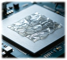
Our graphene originates from carefully selected highly oriented pyrolytic graphite crystals with mosaic spread below 0.4 degrees. Technicians press adhesive tape against a freshly cleaved HOPG surface, peel, fold, and repeat under optical guidance until flakes thin to monolayer and few-layer thicknesses. The tape is then pressed against a silicon wafer with 300 nm thermal oxide, and slow removal leaves graphene flakes adhered to the substrate by van der Waals forces alone.
- Source crystal: HOPG grade A or ZYA, mosaic angle <0.4 deg, verified by X-ray rocking curve.
- Typical flake dimensions: 5 to 50 um lateral size, depending on crystal domain and exfoliation cycle.
- Monolayer confirmation: Raman 2D/G ratio >1.5, D/G <0.1, optical contrast on 300 nm SiO2.
- Transfer options: as-exfoliated on SiO2/Si, or dry/wet transfer to your target substrate.
- Cleanliness: no PMMA residue for as-exfoliated samples; optional annealing at 300-400C in Ar/H2.
Exfoliated h-BN from High-Quality Bulk Crystals
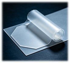
Hexagonal boron nitride is indispensable as a substrate and encapsulant for graphene and TMDC devices. Our h-BN flakes are cleaved from bulk single crystals grown by high-temperature high-pressure methods, yielding starting material with extremely low defect density. Exfoliated h-BN preserves the atomically flat surface that makes it the dielectric of choice for van der Waals heterostructure fabrication.
- Monolayer and few-layer flakes, lateral sizes typically 10 to 40 um.
- Surface roughness <0.15 nm RMS across exfoliated terraces, confirmed by AFM.
- Dielectric breakdown >10 MV/cm for few-layer stacks.
- Available on SiO2/Si or dry-transferred to your target substrate.
TMDC Monolayers from Natural and Synthetic Crystals
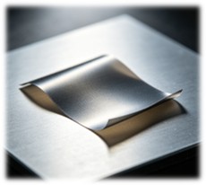
Transition metal dichalcogenides undergo a dramatic electronic transformation when thinned to monolayer thickness: indirect gaps become direct, light emission intensifies by orders of magnitude, and valley-selective optical response emerges. Our mechanically exfoliated TMDCs are sourced from carefully chosen bulk crystals — natural molybdenite for MoS2, physical vapor transport-grown boules for WS2, WSe2, and MoSe2 — and cleaved with the same precision as our graphene.
- MoS2: direct gap 1.8 eV, PL at 1.9 eV, n-type FET behavior, typical flake 10-30 um.
- WS2: strong spin-orbit coupling, valley-selective circular dichroism, PL quantum yield up to 10 percent.
- WSe2: ambipolar transport, p-type dominant with Pd contacts, exciton binding energy ~370 meV.
- MoSe2: electron mobility exceeding MoS2 at room temperature, extended infrared photoresponse.
Few-Layer Black Phosphorus
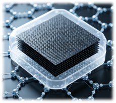
Black phosphorus occupies a unique position in the 2D materials catalog. Its thickness-tunable direct bandgap spans the technologically critical range from 0.3 eV (bulk) to about 2.0 eV (monolayer), bridging the gap between zero-gap graphene and wide-gap TMDCs. Its strong in-plane anisotropy opens device possibilities that isotropic materials cannot match. The challenge is ambient stability, which we address through h-BN encapsulation performed in glovebox environments.
- Source: sublimation-grown bulk BP crystals, purity >99.995 percent.
- Few-layer flakes (2-10 layers) with lateral dimensions 5-20 um.
- Anisotropy ratio ~2:1 between armchair and zigzag transport directions.
- Available h-BN encapsulated for ambient-stable shipping and handling.
Bernal-Stacked Multilayer Graphene
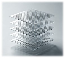
Not every device requires monolayer graphene. Bernal-stacked bilayer and few-layer graphene exhibit electric-field-tunable bandgaps, richer Landau level spectra, and stronger interlayer coupling phenomena than monolayer films. Our multilayer flakes are exfoliated from HOPG with controlled thickness confirmed by Raman and optical contrast, and can be sourced with known twist angles for moire physics studies.
- Bilayer: AB Bernal stacking, bandgap tunable to ~250 meV under dual gating.
- Trilayer and few-layer: ABA and ABC stacking variants, thickness 1-10 nm.
- Twist angle engineering: controlled rotation for moire superlattice devices.
Research Domains That Depend on Exfoliated Single Crystals
The most cited papers in 2D materials science overwhelmingly rely on mechanically exfoliated flakes. The reason is simple: when the physics you seek to observe is subtle — a fractional quantum Hall state, an interlayer exciton resonance, a spin-valley locking signature — any disorder in the starting material can mask or destroy the effect. Representative research programs powered by our exfoliated products include:
- Quantum transport: quantum Hall effect, Shubnikov-de Haas oscillations, fractional states, and ballistic transport in pristine graphene and h-BN heterostructures.
- Twistronics: moire superlattices in twisted bilayer and trilayer graphene, magic-angle flat bands, correlated insulating and superconducting states.
- Valleytronics and spintronics: polarization-selective valley emission in TMDCs, spin-valley locking, 2D magnetic proximity effects.
- Excitonics and quantum light: interlayer excitons in TMDC heterobilayers, single-photon emission from WSe2 defect sites, exciton-polariton condensation.
- Infrared optoelectronics: black phosphorus photodetectors covering the mid-wave infrared, anisotropic absorption for polarimetric imaging.
- Fundamental device prototyping: proof-of-concept FETs, diodes, tunnel transistors, and memory elements where crystal quality matters more than scalability.
Characterization Protocols: What You Receive with Every Flake
We do not ship blind. Every batch of mechanically exfoliated flakes is characterized by our in-house analytical suite, and the data accompanies your delivery. For custom orders, additional characterization can be arranged on request.
- Optical microscopy: color-contrast imaging on 300 nm SiO2 for rapid thickness screening and flake mapping.
- Raman spectroscopy: layer count verification, D/G ratio for defect assessment, 2D/G ratio for monolayer confirmation in graphene.
- Atomic force microscopy: exact thickness measurement, surface roughness quantification, edge profile imaging.
- Photoluminescence spectroscopy: direct gap confirmation for monolayer TMDCs, PL intensity and linewidth reporting.
- Transmission electron microscopy: on request, lattice imaging and selected-area diffraction for crystallinity confirmation.
Tailored Exfoliation: Beyond the Standard Catalog
Standard flakes cover many needs, but frontier research often demands something specific. Perhaps you need graphene on a non-standard oxide thickness for optimized optical visibility. Perhaps you require a particular TMDC heterostructure pre-assembled by dry transfer. Perhaps you want h-BN of a specific thickness range to achieve a target capacitance in a dual-gated device. Our custom exfoliation service accommodates these and other specialized requests.
We have delivered twisted bilayer graphene with specified rotation angles, pre-encapsulated BP flakes sealed in h-BN for air-stable operation, and multi-material stacks combining graphene, h-BN, and MoS2 in a single van der Waals heterostructure. Describe your target device architecture, and our materials team will propose a fabrication protocol, quote a timeline, and produce a characterized prototype batch for your evaluation.
Request Exfoliated Flakes or Discuss a Custom Project
Browse our mechanically exfoliated product catalog, request a characterization data package, or tell us about the specific flake geometry, material stack, or substrate configuration your experiment requires. Our materials scientists will respond with a feasibility assessment and a clear path forward.
| Catalog Number | Product Name | Order | Quantity |
|---|---|---|---|
| DFSC-0001 | Mechanical Exfoliation Tape (12.7 mm × 11.4 m) |
-
+
|
|
| DFSC-0002 | Monolayer Single-Crystal Graphene on SiO2/Si (1 cm × 1 cm, 300 nm SiO2) |
-
+
|
|
| DFSC-0003 | Monolayer Single-Crystal Graphene on SiO2/Si (1 cm × 1 cm, 90 nm SiO2) |
-
+
|
|
| DFSC-0004 | Mechanically Exfoliated WSe2 on SiO2/Si (10 mm × 10 mm) |
-
+
|
|
| DFSC-0005 | Suspended 2D Materials on SiO2 Substrate (1 cm × 1 cm) |
-
+
|
|
| DFSC-0006 | Mechanically Exfoliated MoS2 on SiO2/Si (10 mm × 10 mm) |
-
+
|
|
| DFSC-0007 | Bilayer Single-Crystal Graphene on SiO2/Si (2 cm × 2 cm, 300 nm SiO2) |
-
+
|
|
| DFSC-0008 | Monolayer Single-Crystal Graphene on SiO2/Si (2 cm × 2 cm, 300 nm SiO2) |
-
+
|
|
| DFSC-0009 | Monolayer Single-Crystal Graphene on SiO2/Si (Electronic Grade, 2 cm × 2 cm) |
-
+
|
|
| DFSC-0010 | Monolayer Single-Crystal Graphene on Sapphire (2 cm × 2 cm) |
-
+
|
For Research or Industrial Raw Materials, Not For Personal Medical Use!