

Products
- High-Quality Graphene
- CVD Graphene, Graphene-Like Materials
- Graphene-Like Series
- Defect-Free Single-Crystal Graphene and Graphene-Like Materials (Mechanical Exfoliation)
- Quantum Dot Series
- Aggregation-Induced Emission (AIE)
- Near-Infrared II (NIR-II) Fluorescent Dyes
- Graphdiyne
- Two-Dimensional Transition Metal Carbides/Nitrides/Borides (MXene)
- Metal Nanomaterials and Other Functional Bio-Nanomaterials
- Metal-Organic Frameworks (MOF)
- Covalent Organic Frameworks (COF)
- Two-Dimensional Layered Metal Oxides (LDH)
- Carbon Nanotube Powders, Pastes
- Carbon Nanotube Arrays and Special Carbon Nanotube Materials
- High-Quality Metallic and Semiconducting High-Purity Single-Walled Carbon Nanotubes
- Carbon Nanotube Sponges
- Mesoporous Carbon and Carbon Nanomaterials
- High-Quality Fullerenes
- One-Dimensional Nanomaterials
- Molecular Sieves
- Inorganic Nanomaterials
- Perovskite Materials
- Highly Oriented Pyrolytic Graphite (HOPG)
- Organic Materials
- Single-Atom Catalysts
- Thermoelectric Materials
- Sodium Storage Materials
- Industrial-Grade Nanomaterials
- Solid-State Lithium Batteries
- Hydrogel Series and Consumables
Online Inquiry
Organic Materials
Organic materials occupy a singular position in the world of functional materials. Unlike their inorganic counterparts, which are constrained by the rigid lattice geometries of crystalline solids, organic molecules can be synthesized with an almost infinite variety of shapes, sizes, and electronic structures. Through judicious molecular design — extending conjugated backbones, attaching electron-donating or electron-withdrawing substituents, or introducing steric bulk to suppress aggregation — researchers can tune HOMO and LUMO energy levels with sub-100 meV precision, adjust charge carrier mobilities across five orders of magnitude, and tailor solubility for solution processing or thermal stability for vacuum deposition. This molecular-level programmability has made organic materials the foundation of technologies ranging from OLED displays and organic solar cells to perovskite device charge transport layers and molecular sensing platforms.
Eata Nanomaterials supplies a comprehensive range of high-purity organic materials for research and industrial applications. Our portfolio includes benchmark hole transport materials such as Spiro-OMeTAD and PTAA for perovskite solar cells, n-type and p-type organic semiconductors for thin-film transistors and photovoltaics, phosphorescent and thermally activated delayed fluorescence host and emitter materials for OLEDs, self-assembled monolayer precursors for interface engineering, and a diverse selection of ligands and building blocks for coordination chemistry and supramolecular assembly. All materials are purified by train sublimation, recrystallization, or column chromatography to achieve purities of 99.5% or higher, with characterization by NMR, HPLC, and mass spectrometry provided as standard.
Hole Transport Materials for Perovskite Solar Cells
The hole transport layer in a perovskite solar cell performs a deceptively simple task — extracting photogenerated holes from the perovskite absorber and transporting them to the anode — yet its quality is one of the dominant factors determining both power conversion efficiency and operational stability. Spiro-OMeTAD (2,2',7,7'-tetrakis(N,N-di-p-methoxyphenylamine)-9,9'-spirobifluorene) has remained the benchmark hole transport material for regular n-i-p perovskite devices for over a decade, routinely enabling certified efficiencies exceeding 25%. Its spirobifluorene core enforces an amorphous morphology that forms intimate contact with the perovskite surface, while the four methoxydiphenylamine substituents provide hole-transporting functionality with a HOMO level well-aligned to the valence band of MAPbI3. Hole transfer from perovskite to Spiro-OMeTAD occurs on picosecond timescales, four orders of magnitude faster than to many polymer alternatives, making it the material of choice for researchers pursuing record efficiency.
PTAA (poly[bis(4-phenyl)(2,4,6-trimethylphenyl)amine]) offers a compelling alternative, particularly for inverted p-i-n architectures where its ability to form exceptionally thin, pinhole-free films enables high fill factors without the aging period required by Spiro-OMeTAD. High molecular weight PTAA (Mw > 50 kDa) suppresses interfacial recombination more effectively than Spiro-OMeTAD, contributing to higher open-circuit voltages in optimized devices. Both materials require p-doping for optimal performance: LiTFSI with tBP is the classic combination for Spiro-OMeTAD, while tris(pentafluorophenyl)borane (BCF) has emerged as a superior dopant for PTAA that improves junction quality and eliminates the moisture-seeking lithium ions that plague long-term stability. We supply Spiro-OMeTAD, PTAA, and the full suite of dopants — LiTFSI, tBP, BCF, and F4-TCNQ — as individual components or pre-mixed formulations.
 Amber glass vials containing high-purity organic semiconductor powders of various colors for charge transport layer applications
Organic Semiconductors for Thin-Film Transistors and Photovoltaics
Organic field-effect transistors (OFETs) form the backbone of flexible electronics — the switch arrays that drive e-paper displays, the sensor backplanes in wearable health monitors, and the logic circuits in radio-frequency identification tags. The performance of these devices depends critically on the organic semiconductor that forms the channel: p-type materials such as pentacene, DNTT, and 2,7-dioctyl[1]benzothieno[3,2-b][1]benzothiophene (C8-BTBT) transport holes, while n-type materials such as PTCDI-C8, N2200, and perylene diimide derivatives transport electrons. The highest-performing small-molecule OFETs now achieve hole mobilities above 10 cm^2 V^-1 s^-1 in carefully optimized films, approaching the performance of amorphous silicon and enabling practical circuit operation.
In organic photovoltaics, donor-acceptor bulk heterojunction blends have achieved certified power conversion efficiencies exceeding 19% in single-junction cells and 20% in tandem configurations with perovskite top cells. Our catalog includes classic donor polymers such as P3HT, PTB7-Th, and PM6; fullerene acceptors including PCBM and ICBA; and the non-fullerene acceptors — ITIC, Y6, and L8-BO — that have driven the recent surge in OPV efficiency. For researchers seeking to optimize blend morphology, we supply these materials across a range of molecular weights, regioregularities, and end-group functionalizations that directly influence film microstructure and device performance.
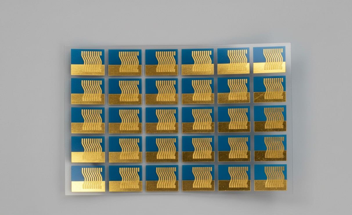 Array of organic thin-film transistor devices fabricated on a flexible transparent substrate with gold source and drain electrodes
OLED Host and Emitter Materials
Organic light-emitting diodes have transformed display technology, and the materials that make them possible are among the most refined organic semiconductors ever developed. The ideal OLED host material must simultaneously transport both electrons and holes, confine excitons on the guest emitter through a wider bandgap, and form stable, pinhole-free thin films at temperatures compatible with device processing. Our catalog includes benchmark host materials such as mCP (1,3-bis(N-carbazolyl)benzene) for blue and green phosphorescent emitters, TCTA (tris(4-carbazoyl-9-ylphenyl)amine) for hole-dominated devices, and CBP (4,4'-bis(N-carbazolyl)-1,1'-biphenyl) as a versatile wide-bandgap host.
For emitters, we supply phosphorescent iridium complexes — Ir(ppy)3 for green emission, Ir(MDQ)2(acac) for red, and FIrpic for blue — that harvest both singlet and triplet excitons through strong spin-orbit coupling, enabling internal quantum efficiencies approaching unity. Thermally activated delayed fluorescence (TADF) emitters represent the next frontier: all-organic molecules such as 4CzIPN that upconvert triplet excitons to singlets through reverse intersystem crossing, eliminating the need for rare and expensive iridium while maintaining high efficiency. Whether your application demands the proven performance of phosphorescence or the sustainability promise of TADF, our emitter materials deliver the purity and reproducibility required for device-grade fabrication.
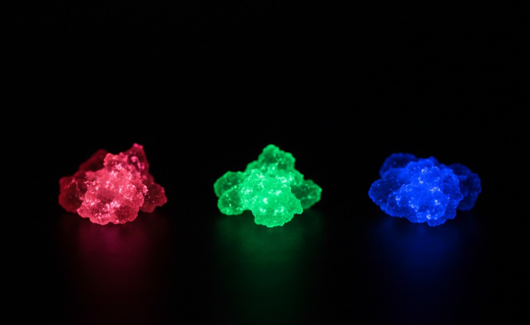 Organic phosphorescent OLED emitter materials exhibiting vivid red, green, and blue luminescence under UV excitation
Self-Assembled Monolayers for Interface Engineering
Self-assembled monolayers (SAMs) have emerged as one of the most impactful developments in device interface engineering. These single-molecule-thick films form spontaneously when a substrate is immersed in a dilute solution of molecules bearing a surface-reactive head group — carboxylic acids for metal oxides, phosphonic acids for a broader range of surfaces, or silanes for silica. The result is a precisely oriented monolayer that modifies the work function, improves wettability, and introduces chemical functionality at the interface between two device layers.
In perovskite solar cells, SAMs have displaced thicker organic transport layers in the most efficient inverted devices. Me-4PACz ((4-(3,6-dimethyl-9H-carbazol-9-yl)butyl)phosphonic acid) and 2PACz (2-(9H-carbazol-9-yl)ethyl)phosphonic acid) form tightly packed monolayers on indium tin oxide that efficiently extract holes while eliminating the parasitic absorption and series resistance of conventional polymer or small-molecule hole transport layers. Devices incorporating these SAMs have achieved certified efficiencies exceeding 25% in inverted architectures. We supply Me-4PACz, 2PACz, and related phosphonic acid-functionalized carbazole derivatives with the high purity and defined anchor group orientation required for reproducible device performance.
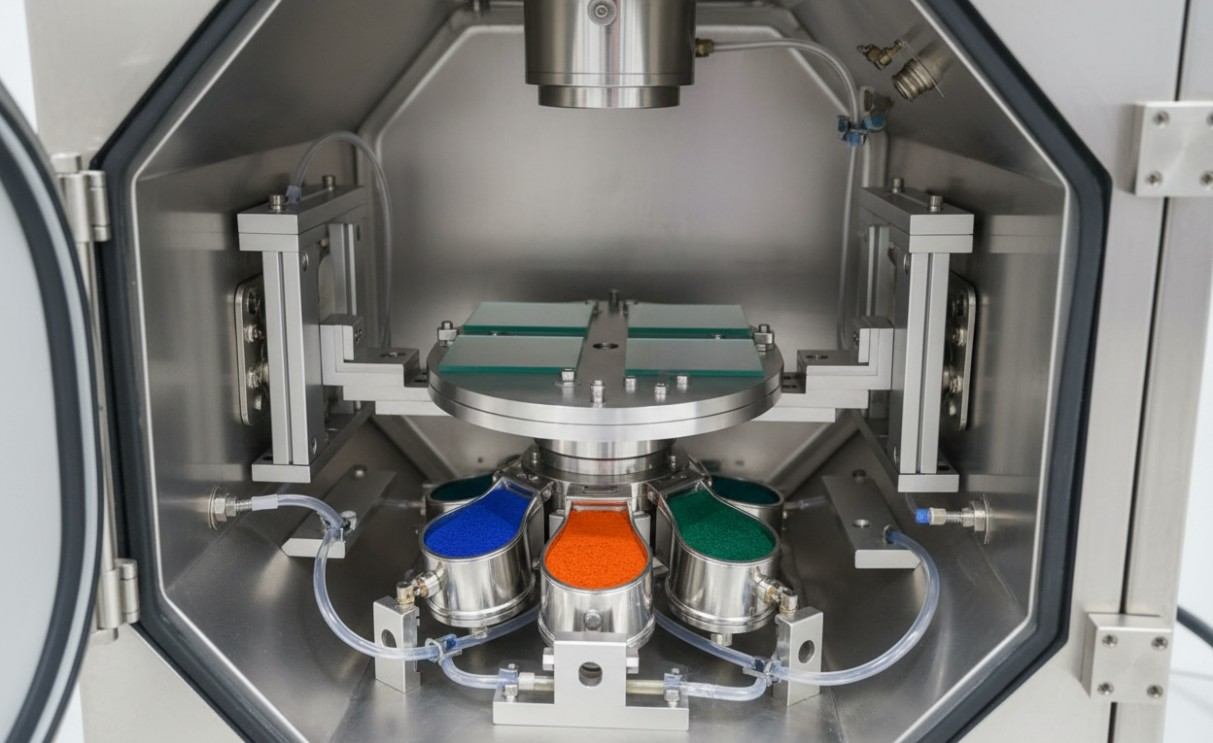 Vacuum thermal evaporation chamber for depositing organic semiconductor thin films with multiple effusion cells and substrate holder
Organic Ligands and Functional Building Blocks
Beyond charge transport and emission, organic molecules serve as the molecular scaffolds that organize inorganic nanomaterials into functional architectures. Bipyridine and phenanthroline ligands coordinate transition metal ions in dye-sensitized solar cells and photocatalytic systems. Phosphine ligands — triphenylphosphine, TOPO, and oleylamine — stabilize colloidal quantum dots during synthesis and prevent aggregation in solution. Carboxylic acid and thiol-terminated molecules anchor nanoparticles to electrodes and enable electronic coupling between adjacent nanocrystals in thin-film devices.
Our catalog of organic ligands and building blocks encompasses bipyridines (2,2'-bipyridine, 4,4'-dimethyl-2,2'-bipyridine), phenanthrolines (1,10-phenanthroline, bathophenanthroline), phosphines (triphenylphosphine, trioctylphosphine), amines (oleylamine, octylamine), and thiols (1-hexanethiol, 1-dodecanethiol) for surface functionalization. For supramolecular chemistry and metal-organic framework construction, we supply dicarboxylic acids (terephthalic acid, trimesic acid), imidazoles, and porphyrins. All ligands are purified to remove metal contaminants that would interfere with sensitive catalytic or electronic applications, and are available in gram to kilogram quantities.
 Schlenk line setup for handling air-sensitive organic compounds with vacuum and inert gas connections
Featured Products
| Search Term | Specifications | Applications |
| Spiro-OMeTAD | Purity >99.5%; Sublimed grade; CAS 207739-72-8 | Perovskite HTL, >25% PCE |
| PTAA | Mw >50 kDa; Amorphous; HOMO: -5.2 eV | Inverted PSCs, flexible devices |
| BCF dopant | CAS 1109-15-5; Lewis acid p-dopant | Alternative to LiTFSI for PTAA |
| Me-4PACz / 2PACz | Phosphonic acid SAM; Monolayer | Inverted PSC interface, >25% PCE |
| OLED host (mCP/CBP) | Wide bandgap; Triplet energy >2.9 eV | Phosphorescent OLEDs |
| Ir(ppy)3 / 4CzIPN | Phosphorescent/TADF emitter; QY >90% | High-efficiency displays |
| PM6 / Y6 / L8-BO | NF-acceptor; OPV blend >19% PCE | Organic photovoltaics |
| C8-BTBT / DNTT | Small molecule; Hole mobility >10 cm2/Vs | Flexible OFET circuits |
Applications Across Research and Industry
Perovskite Solar Cells: Spiro-OMeTAD and PTAA serve as benchmark hole transport layers, while SAM precursors enable >25% efficiency in inverted architectures with minimal parasitic absorption.
Organic Photovoltaics: Donor polymers (PM6, PTB7-Th) and non-fullerene acceptors (Y6, L8-BO) in bulk heterojunction blends achieve >19% PCE in single-junction cells.
OLED Displays: Phosphorescent iridium complexes and TADF emitters in wide-bandgap hosts deliver near-unity internal quantum efficiency for high-brightness, wide-color-gamut displays.
Flexible Electronics: High-mobility small-molecule semiconductors (C8-BTBT, DNTT) in OFET arrays drive the backplanes of foldable displays and wearable sensors.
Quantum Dot Functionalization: Phosphine, amine, and thiol ligands control nanocrystal size during synthesis, stabilize colloidal dispersions, and mediate electronic coupling in device films.
Interface Engineering: SAMs with phosphonic acid anchor groups modify work functions and introduce chemical functionality at metal oxide and transparent conductor surfaces.
Quality Assurance and Purification
The performance of organic electronic devices is exquisitely sensitive to trace impurities — residual solvent molecules trapped in films, metal ions from catalysts used in synthesis, or isomeric contaminants with subtly different electronic properties. Recognizing this, we subject every organic material to a rigorous purification and characterization protocol. Small molecules are purified by train sublimation under high vacuum, achieving residual metal contents below 1 ppm and organic purity exceeding 99.5% as verified by HPLC. Polymers are purified by sequential Soxhlet extraction to remove oligomers and catalyst residues, followed by precipitation to fractionate by molecular weight. Characterization includes proton and carbon-13 NMR spectroscopy for structural verification, gel permeation chromatography for polymer molecular weight determination, thermogravimetric analysis for thermal stability assessment, cyclic voltammetry for HOMO/LUMO level determination, and differential scanning calorimetry for thermal transition identification. All data accompany the material in a comprehensive certificate of analysis.
Custom Synthesis and Molecular Design
The molecular tunability of organic materials is their greatest strength, and we leverage this flexibility through our custom synthesis program. Our capabilities include end-group modification of oligothiophenes and perylene diimides to tune solubility and crystallinity; deuteration of aromatic cores to improve OLED operational lifetime through suppression of vibrational quenching; synthesis of novel SAM precursors with custom anchor groups and functional head groups for specific substrate chemistries; preparation of donor-acceptor copolymers with tailored optical bandgaps for tandem solar cell applications; and scale-up of literature materials from milligram proof-of-concept to multi-gram device fabrication batches. Whether you need a literature compound reproduced at higher purity, a known structure modified for a new application, or an entirely novel molecule designed and synthesized from scratch, our organic chemistry team is equipped to deliver.
Contact Us— Reach out to Eata Nanomaterials to discuss your organic material requirements, request product samples, or explore custom synthesis and molecular design services for your research or device development program.
| Catalog Number | Product Name | Order | Quantity |
|---|---|---|---|
| ORGM-0001 | PEDOT:PSS High Transparency Electronic 01 |
-
+
|
|
| ORGM-0002 | PEDOT:PSS High Transparency Electronic 02 |
-
+
|
|
| ORGM-0003 | PEDOT:PSS High Transparency Electronic 03 |
-
+
|
|
| ORGM-0004 | PEDOT/PSS Conductive Polymer Water Dispersion 01 |
-
+
|
|
| ORGM-0005 | PEDOT/PSS Conductive Polymer Water Dispersion 02 |
-
+
|
|
| ORGM-0006 | Gel Electrolyte |
-
+
|
|
| ORGM-0007 | PANI:PSS Polyaniline Aqueous Dispersion (~1.23% solid content) |
-
+
|
|
| ORGM-0008 | PANI:PSS Polyaniline Aqueous Dispersion (~5% solid content) |
-
+
|
|
| ORGM-0009 | Stretched PEDOT Conductive Ink |
-
+
|
|
| ORGM-0010 | SFX-2,7-DDPA (N2,N2,N7,N7-Tetraphenylspiro[fluorene-9,9'-xanthene]-2,7-diamine) |
-
+
|
For Research or Industrial Raw Materials, Not For Personal Medical Use!